NEET Exam  >  NEET Tests  >  Physics 31 Years NEET Chapterwise Solved Papers  >  31 Year NEET Previous Year Questions: Semiconductor Electronics - 2 - NEET MCQ

31 Year NEET Previous Year Questions: Semiconductor Electronics - 2 - NEET MCQ


Test Description

25 Questions MCQ Test Physics 31 Years NEET Chapterwise Solved Papers - 31 Year NEET Previous Year Questions: Semiconductor Electronics - 2

31 Year NEET Previous Year Questions: Semiconductor Electronics - 2 for NEET 2025 is part of Physics 31 Years NEET Chapterwise Solved Papers preparation. The 31 Year NEET Previous Year Questions: Semiconductor Electronics - 2 questions and answers have been prepared according to the NEET exam syllabus.The 31 Year NEET Previous Year Questions: Semiconductor Electronics - 2 MCQs are made for NEET 2025 Exam. Find important definitions, questions, notes, meanings, examples, exercises, MCQs and online tests for 31 Year NEET Previous Year Questions: Semiconductor Electronics - 2 below.
Solutions of 31 Year NEET Previous Year Questions: Semiconductor Electronics - 2 questions in English are available as part of our Physics 31 Years NEET Chapterwise Solved Papers for NEET & 31 Year NEET Previous Year Questions: Semiconductor Electronics - 2 solutions in Hindi for Physics 31 Years NEET Chapterwise Solved Papers course. Download more important topics, notes, lectures and mock test series for NEET Exam by signing up for free. Attempt 31 Year NEET Previous Year Questions: Semiconductor Electronics - 2 | 25 questions in 50 minutes | Mock test for NEET preparation | Free important questions MCQ to study Physics 31 Years NEET Chapterwise Solved Papers for NEET Exam | Download free PDF with solutions
31 Year NEET Previous Year Questions: Semiconductor Electronics - 2 - Question 1

Reverse bias applied to a junction diode [2003]

Detailed Solution for 31 Year NEET Previous Year Questions: Semiconductor Electronics - 2 - Question 1

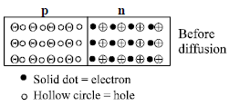
In reverse biasing, the conduction across the
p-n junction does not take place due to
majority carriers but takes place due to
minority carriers if the voltage of external
battery is large. The size of the depletion
region increases thereby increasing the
potential barrier.

31 Year NEET Previous Year Questions: Semiconductor Electronics - 2 - Question 2

In semiconductors, at room temperature [2004]

Detailed Solution for 31 Year NEET Previous Year Questions: Semiconductor Electronics - 2 - Question 2

In a semiconductor, at room temperature, few of the electrons in the valence band gain enough energy to jump into the conduction band whereas the others remain in the valence band. Hence, the valence band is partially empty and the conduction band is partially filled.

31 Year NEET Previous Year Questions: Semiconductor Electronics - 2 - Question 3

The peak voltage in the output of a half-wavediode rectifier fed with a sinusoidal signalwithout filter is 10V. The d.c. component of theoutput voltage is [2004]

Detailed Solution for 31 Year NEET Previous Year Questions: Semiconductor Electronics - 2 - Question 3

31 Year NEET Previous Year Questions: Semiconductor Electronics - 2 - Question 4

The output of OR gate is 1  [2004]

Detailed Solution for 31 Year NEET Previous Year Questions: Semiconductor Electronics - 2 - Question 4

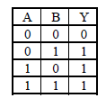
Output will be one if A or B or both are one.
Y= A + B

31 Year NEET Previous Year Questions: Semiconductor Electronics - 2 - Question 5

In a p-n junction photocell, the value of thephoto-electromotive force produced bymonochromatic light is proportional to [2004]

Detailed Solution for 31 Year NEET Previous Year Questions: Semiconductor Electronics - 2 - Question 5

Electromotive force depends upon intensity
of light falling, it does not depend on
frequency of barrier voltage

31 Year NEET Previous Year Questions: Semiconductor Electronics - 2 - Question 6

Of the diodes shown in following diagrams, which one is reverse biased ? [2004]

Detailed Solution for 31 Year NEET Previous Year Questions: Semiconductor Electronics - 2 - Question 6

Positive terminal is at lower potential (0V)
and negative terminal is at higher potential
+5 V

31 Year NEET Previous Year Questions: Semiconductor Electronics - 2 - Question 7

Choose the only false statement from thefollowing [2005]

Detailed Solution for 31 Year NEET Previous Year Questions: Semiconductor Electronics - 2 - Question 7

(a) is true as in case of conductors either the
conduction & valence band overlap or
conduction band is partially filled.
(b) is true as insulators have energy gap of
the order of 5 to 10 eV.
(c) is false as resistivity (opposite of
conductivity) decreases with increase in
temperature.
(d) is true as with increase in temperature
more and more electrons jump to the
conduction band. So, conductivity increases.

31 Year NEET Previous Year Questions: Semiconductor Electronics - 2 - Question 8

Carbon, silicon and germanium atoms have fourvalence electrons each. Their valence andconduction bands are separated by energy bandgaps represented by (Eg)C, (Eg)Si and (Eg)Gerespectively. Which one of the followingrelationships is true in their case? [2005]

Detailed Solution for 31 Year NEET Previous Year Questions: Semiconductor Electronics - 2 - Question 8

Due to strong electronegativity of carbon

31 Year NEET Previous Year Questions: Semiconductor Electronics - 2 - Question 9

Application of a forward bias to a p–n junction [2005]

Detailed Solution for 31 Year NEET Previous Year Questions: Semiconductor Electronics - 2 - Question 9

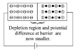
In forward bias, p-type is connected to positive terminal of battery and n-type is connected to negative terminal of battery. Hence, carriers are accelerated towards opposite terminals for the conduction thereby increases the number of electrons on n-side.

Number of donor s is more because
electrons from –ve terminal of the cell
pushes (enters) the n side and decreases
the number of uncompensated pentavalent
ion due to which potential barrier is
reduced. The neutralised pentavalent atom
are again in position to donate electrons.

31 Year NEET Previous Year Questions: Semiconductor Electronics - 2 - Question 10

Zener diode is used for [2005]

Detailed Solution for 31 Year NEET Previous Year Questions: Semiconductor Electronics - 2 - Question 10

At a certain reverse bias voltage, zener diode
allows current to flow through it and hence
maintains the voltage supplied to any load
Hence, it is used for stabilisation.

31 Year NEET Previous Year Questions: Semiconductor Electronics - 2 - Question 11

The following figure shows a logic gate circuit with two inputs A and B and the output C. The voltage waveforms of A, B and C are as shown below

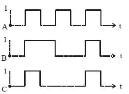
The logic circuit gate is [2006]

Detailed Solution for 31 Year NEET Previous Year Questions: Semiconductor Electronics - 2 - Question 11

On the basis of given graph, following table
is possible.

It is the truth table of AND gate.

31 Year NEET Previous Year Questions: Semiconductor Electronics - 2 - Question 12

A transistor is operated in common emitterconfiguration at constant collector voltage Vc =1.5V such that a change in the base current from100 μA to 150 μA produces a change in thecollector current from 5 mA to 10 mA. The currentgain (β) is [2006]

Detailed Solution for 31 Year NEET Previous Year Questions: Semiconductor Electronics - 2 - Question 12

31 Year NEET Previous Year Questions: Semiconductor Electronics - 2 - Question 13

A forward biased diode is     [2006]

Detailed Solution for 31 Year NEET Previous Year Questions: Semiconductor Electronics - 2 - Question 13

In forward biasing of a diode, the emitted
should be at a higher potential, Here, only in
option (c) emitter is at higher potential with
bias voltage 0V compared to the collector,
which is at –2V. So, it is reverse biased.

31 Year NEET Previous Year Questions: Semiconductor Electronics - 2 - Question 14

The radius of germanium (Ge) nuclide ismeasured to be twice the radius of 94Be . Thenumber of nucleons in Ge are [2006]

Detailed Solution for 31 Year NEET Previous Year Questions: Semiconductor Electronics - 2 - Question 14

We use the formula,
R = R0 A1/3
This represents relation between atomic mass
and radius of the nucleus.

31 Year NEET Previous Year Questions: Semiconductor Electronics - 2 - Question 15

In the following circuit, the output Y for all possible inputs A and B is expressed by the truth table [2007]

Detailed Solution for 31 Year NEET Previous Year Questions: Semiconductor Electronics - 2 - Question 15

Therefore truth table :

31 Year NEET Previous Year Questions: Semiconductor Electronics - 2 - Question 16

A common emitter amplifier has a voltage gainof 50, an input impedance of 100Ω and an outputimpedance of 200Ω. The power gain of theamplifier is [2007]

Detailed Solution for 31 Year NEET Previous Year Questions: Semiconductor Electronics - 2 - Question 16

31 Year NEET Previous Year Questions: Semiconductor Electronics - 2 - Question 17

For a cubic crystal structure which one of thefollowing relations indicating the cellcharacteristics is correct? [2007]

Detailed Solution for 31 Year NEET Previous Year Questions: Semiconductor Electronics - 2 - Question 17

For a cubic crystal,
a = b = c and α = β = γ = 90°

31 Year NEET Previous Year Questions: Semiconductor Electronics - 2 - Question 18

In the energy band diagram of a material shown below, the open circles and filled circles denote holes and electrons respectively. The material is   [2007]
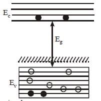
Detailed Solution for 31 Year NEET Previous Year Questions: Semiconductor Electronics - 2 - Question 18

For a p-type semiconductor, the acceptor
energy level, as shown in the diagram, is
slightly above the top Ev of the valence band.
With very small supply of energy an electron
from the valence band can jump to the level
EA and ionise acceptor negatively.

31 Year NEET Previous Year Questions: Semiconductor Electronics - 2 - Question 19

The voltage gain of an amplifier with 9% negativefeedback is 10. The voltage gain withoutfeedback will be [2008]

Detailed Solution for 31 Year NEET Previous Year Questions: Semiconductor Electronics - 2 - Question 19

Negative feedback is applied to reduce the
output voltage of an amplifier. If there is no
negative feedback, the value of output
voltage could be very high. In the options
given, the maximum value of voltage gain is
100. Hence it is the correct option.

31 Year NEET Previous Year Questions: Semiconductor Electronics - 2 - Question 20

A p-n photodiode is made of a material with aband gap of 2.0 eV. The minimum frequency ofthe radiation that can be absorbed by the materialis nearly [2008]

Detailed Solution for 31 Year NEET Previous Year Questions: Semiconductor Electronics - 2 - Question 20

Eg = 2.0 eV = 2 × 1.6 × 10–19 J
Eg = hv

31 Year NEET Previous Year Questions: Semiconductor Electronics - 2 - Question 21

The circuit

is equivalent to

Detailed Solution for 31 Year NEET Previous Year Questions: Semiconductor Electronics - 2 - Question 21

Let A and B be inputs and Y the output

Then Y1 

Hence, the given circuit is equivalent to a
NOR gate.

31 Year NEET Previous Year Questions: Semiconductor Electronics - 2 - Question 22

The symbolic representation of four logic gates are given below : [2009]

The logic symbols for OR, NOT and NAND gates are respectively:

Detailed Solution for 31 Year NEET Previous Year Questions: Semiconductor Electronics - 2 - Question 22

(iv), (ii), (i)

Option (iii) represents AND gate.

31 Year NEET Previous Year Questions: Semiconductor Electronics - 2 - Question 23

A p-n photodiode is fabricated from a semiconductor with a band gap of 2.5 eV. It candetect a signal of wavelength [2009]

Detailed Solution for 31 Year NEET Previous Year Questions: Semiconductor Electronics - 2 - Question 23

The wavelength detected by photodiode
should be less than λmax. Hence it can
detect a signal of wavelength 4000Å.

31 Year NEET Previous Year Questions: Semiconductor Electronics - 2 - Question 24

A transistor is operated in common-emitterconfiguration at Vc = 2 V such that a change inthe base current from 100 μA to 200 μA producesa change in the collector current from 5 mA to10 mA. The current gain is [2009]

Detailed Solution for 31 Year NEET Previous Year Questions: Semiconductor Electronics - 2 - Question 24

31 Year NEET Previous Year Questions: Semiconductor Electronics - 2 - Question 25

The number of beta particles emitted by aradioactive substance is twice the number ofalpha particles emitted by it. The resultingdaughter is an [2009]

Detailed Solution for 31 Year NEET Previous Year Questions: Semiconductor Electronics - 2 - Question 25

Isotopes of an element have the same atomic
number but different mass number. A
radioactive substance when emits one alpha
particles  its mass number reduces
by 4 and charge no. reduces by 2 and after
emission of two β-particles its charge no.
increase by 2 thus the charge no. i.e. atomic
number remains the same.

28 docs|47 tests
Information about 31 Year NEET Previous Year Questions: Semiconductor Electronics - 2 Page
In this test you can find the Exam questions for 31 Year NEET Previous Year Questions: Semiconductor Electronics - 2 solved & explained in the simplest way possible. Besides giving Questions and answers for 31 Year NEET Previous Year Questions: Semiconductor Electronics - 2, EduRev gives you an ample number of Online tests for practice
Download as PDF