IIT JAM Physics Mock Test - 9 Free Online Test 2026
Full Mock Test & Solutions: IIT JAM Physics Mock Test - 9 (60 Questions)
You can boost your Physics 2026 exam preparation with this IIT JAM Physics Mock Test - 9 (available with detailed solutions).. This mock test has been designed with the analysis of important topics, recent trends of the exam, and previous year questions of the last 3-years. All the questions have been designed to mirror the official pattern of Physics 2026 exam, helping you build speed, accuracy as per the actual exam.
Mock Test Highlights:
- - Format: Multiple Choice Questions (MCQ)
- - Duration: 180 minutes
- - Total Questions: 60
- - Analysis: Detailed Solutions & Performance Insights
Sign up on EduRev for free and get access to these mock tests, get your All India Rank, and identify your weak areas to improve your marks & rank in the actual exam.

In a common emitter amplifier, the unbypassed emitter resistance provide:-
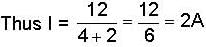
Detailed Solution: Question 1
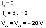
In the following given circuit, calculate the value of "Vce" if the transistor is working in cut off:-

Detailed Solution: Question 2

A change in the value of the emitter resistance (Re), in a differential amplifier:-
Detailed Solution: Question 3
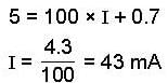
The ripple factor of a power supply is given by (symbols have the usual meaning)
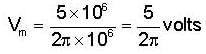
Detailed Solution: Question 4
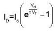
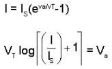
A diode has a reverse saturation current Is = 10-10 A & non-ideality factor η = 2. If diode voltage is 0.9 V then diode current is:-
Detailed Solution: Question 5
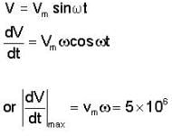
An op-amp has a slow-rate 5V/μs. The largest sinwave output voltage possible at a frequency of 1MHz is:-
Detailed Solution: Question 6
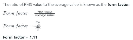
The form factor (in case of resistive load) for a full wave rectifier is:-
Detailed Solution: Question 7
The static characteristic of an adequately forward biased p-n junction is a straight line, if the plot is of:
Detailed Solution: Question 8
Detailed Solution: Question 9
Silicon diode is less suited for low voltage rectifier operation, because:-
Detailed Solution: Question 10
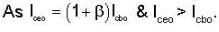
The breakdown voltage of a transistor with its base open is BVCEO & that with emitter open is BVCBO, then
Detailed Solution: Question 11
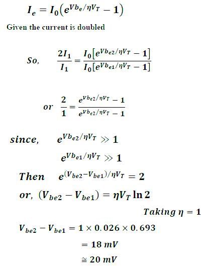
In a bipolar transistor at room temperature, if the emitter current is doubled the voltage across its base emitter junction will
Detailed Solution: Question 12
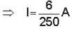
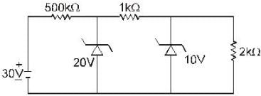
What is the current through 100Ω resistance is the circuit shown below?
Detailed Solution: Question 13

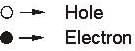
Which of the following statements if not true regarding the magnitude of barrier potential of a p-n junction.
Detailed Solution: Question 14
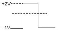
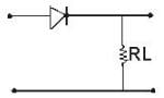
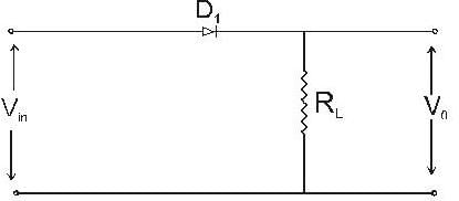
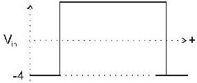
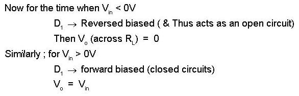
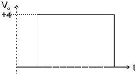
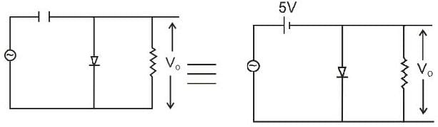
If in a p-n junction diode, a square input signal of 6V is applied see figure be-low, what is the value of the output signal across 'RL'?
Detailed Solution: Question 15
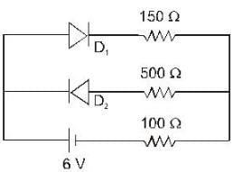
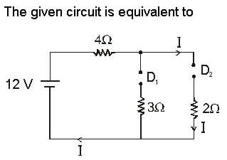
The circuit shown below has two oppositely connected ideal diodes in parallel. What is the current flowing in the circuit?
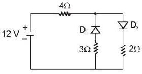
Detailed Solution: Question 16
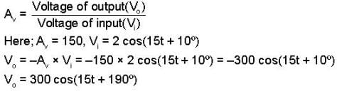
The input signal given to a CE amplifier having a voltage gain of 150 is V1 = 2cos(15t+100). The corresponding output signal is:
Detailed Solution: Question 17
In the following circuit, the voltage across & the current through the 2kΩ resistance are:
Detailed Solution: Question 18

In the following circuit Tr1 & Tr2 are identical transistors having VBE = 0.7V. The current passing through the transistor Tr2 is :
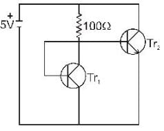
Detailed Solution: Question 19
A bipolar junction transistors with one junction forward biased & either the collector or emitter open, operated in the :
Detailed Solution: Question 20
A silicon diode is in series with a 1.0 kΩ resistor and a 5V battery. If the anode is connected to the positive battery terminal, the cathode voltage with respect to the negative battery terminal is:
Detailed Solution: Question 21
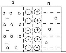
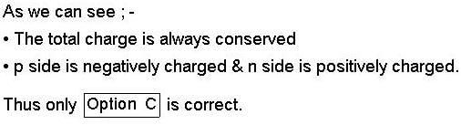
Which one of the following statement is true for a semiconductor p-n junction with no external bias?
Detailed Solution: Question 22
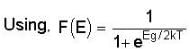
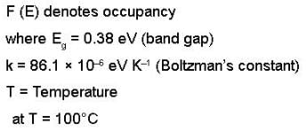
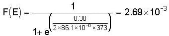
An intrinsic semiconducting sample has an energy gap of 0.38 eV; calculate the probability at 100°C that the lowest level in the conduction band will be occupied.
Detailed Solution: Question 23
Which of the following output curves correctly represent the output of the given clamper circuit:-
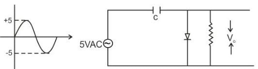
Detailed Solution: Question 24
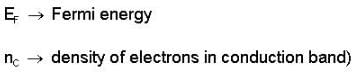
Which relation is correct for intrinsic semiconductor?
(where  conducting of material μn and μp is the electron mobility and hole mobility respectively.
(where
conducting of material μn and μp is the electron mobility and hole mobility respectively.Detailed Solution: Question 25
If the transistor of an amplifier is changed & the gain is increased by two times, which of the following Parameters will have the higher increase in its value :-
Detailed Solution: Question 26
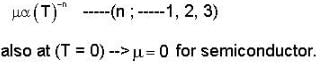
Mobility of free electrons depends on temperature variation in case of a semiconductor as:-
Detailed Solution: Question 27
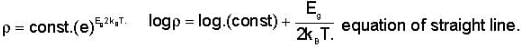
The graph of  where P → Resistinity & 'T' is the temperature :-
where P → Resistinity & 'T' is the temperature :-Detailed Solution: Question 28
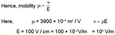
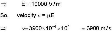
In a germanium semiconductor material used in transistors, mobility of electrons is 3900 cm2N. How much velocity do they have?
Detailed Solution: Question 29
A CE amplifier has voltage gain of 50, an input impedance of 1000Ω and an output impedance of 200Ω. The power gain of the amplifier will be :
Detailed Solution: Question 30

4 docs|21 tests |