ISRO Scientist ECE Electronics Mock Test - 3 Free Online Test 2026
Full Mock Test & Solutions: ISRO Scientist Electronics Mock Test - 3 (95 Questions)
You can boost your Electronics and Communication Engineering (ECE) 2026 exam preparation with this ISRO Scientist Electronics Mock Test - 3 (available with detailed solutions).. This mock test has been designed with the analysis of important topics, recent trends of the exam, and previous year questions of the last 3-years. All the questions have been designed to mirror the official pattern of Electronics and Communication Engineering (ECE) 2026 exam, helping you build speed, accuracy as per the actual exam.
Mock Test Highlights:
- - Format: Multiple Choice Questions (MCQ)
- - Duration: 120 minutes
- - Total Questions: 95
- - Analysis: Detailed Solutions & Performance Insights
- - Sections covered: Discipline, Aptitude
Sign up on EduRev for free and get access to these mock tests, get your All India Rank, and identify your weak areas to improve your marks & rank in the actual exam.

The total equivalent capacitance of the series parallel combination of capacitors across A and B shown in figure is
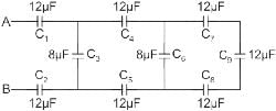
Detailed Solution: Question 1
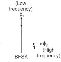
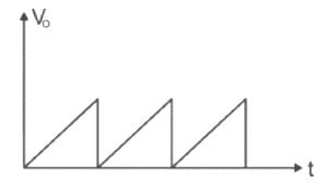
The given waveform describes operation of ______.
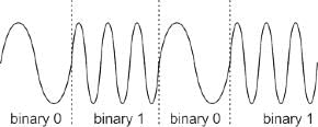
Detailed Solution: Question 2

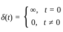
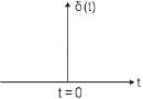
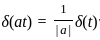
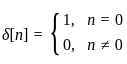
Which of the following points CANNOT be observed about a unit impulse function if it is assumed in the form of a pulse?
Detailed Solution: Question 3

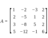
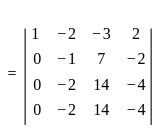
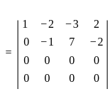
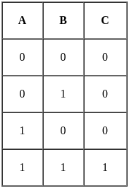
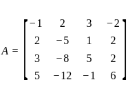 , then the rank of the matrix A is
Detailed Solution: Question 4
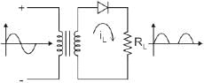
What is the output of a half wave rectifier (in V) when it is supplied with a voltage which has peak value of 12.5 V?
Detailed Solution: Question 5
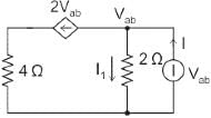
The Thevenin equivalent resistance (RTh) for the circuit shown in fig. is:
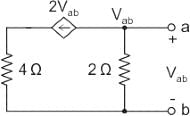
Detailed Solution: Question 6
Which of the following combination is representing an SCR?
Detailed Solution: Question 7
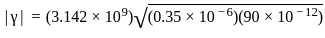
For a lossless transmission line L = 0.35 μH/m, C = 90 pF/m and frequency = 500 MHz. Then the magnitude of propagation constant is
Detailed Solution: Question 8


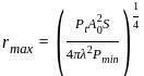
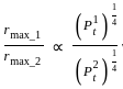
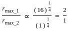
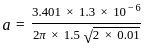
Two radars are transmitting powers P1 and P2. If the transmitted power P1 is 16 times the transmitted power P2 and all other parameters are same then ratio of maximum range of radar 1 to radar 2 is:
Detailed Solution: Question 9
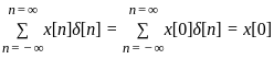
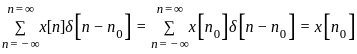
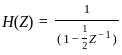
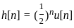 (u[n] is unit step pulses)
this system works as which type of filter?
(u[n] is unit step pulses)Detailed Solution: Question 10

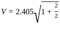
Find the maximum possible core diameter which allows single_mode operation at a wavelength of 1.3 μm in a graded-index fiber having a parabolic refractive index profile core with core refractive index at the core axis of 1.5 and relative index difference of 1%.
Detailed Solution: Question 11


Consider a closed surface S surrounding a volume V. If  is the position vector of a point inside S, with
  the unit normal on S, the value of the integral
  is
is
is the position vector of a point inside S, with the unit normal on S, the value of the integral isDetailed Solution: Question 12
 is the position vector of a point inside a closed surface.
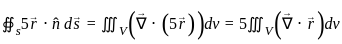
Consider a signal x (t) = 5 cos (2πt/3), + 9 sin (0.5π t) + 3 sin  + 12. Identify the valid statement for x (t).
+ 12. Identify the valid statement for x (t).Detailed Solution: Question 13

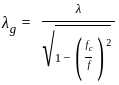
An air-filled rectangular waveguide R1 is operating at the frequency 2 GHz and another air-filled rectangular waveguide R2 is operating at 4 GHz. The guide wavelengths of these waveguides at their respective frequencies are equal. If the cut-off frequency of waveguide R1 is 1 GHz, what is the cut-off frequency of the waveguide R2 in GHz?
Detailed Solution: Question 14
 ; where
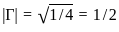
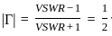
A lossless transmission line is terminated by a load which reflects a part of the incident power. If percentage of the power that is transmitted is 75%, what is value of VSWR is ______.
Detailed Solution: Question 15
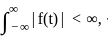
Which of the following statements regarding Laplace and Fourier transforms are correct?
A. In order for a function to possess a Laplace transform, it must obey the condition 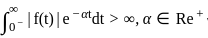
B. In order for a function to possess a Laplace transform, it must obey the condition 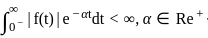
C. For a function to have a Fourier transform, it must obey the condition 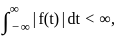
D. For a function to have a Fourier transform, it must obey the condition 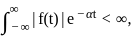
Choose the correct answer from the options given below:
A. In order for a function to possess a Laplace transform, it must obey the condition
B. In order for a function to possess a Laplace transform, it must obey the condition
C. For a function to have a Fourier transform, it must obey the condition
D. For a function to have a Fourier transform, it must obey the condition
Choose the correct answer from the options given below:
Detailed Solution: Question 16
 to
to 

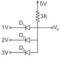
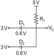
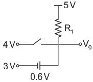
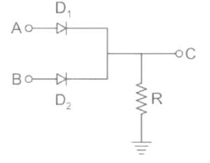
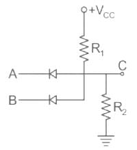
Consider the AND logic circuit in which V2 = 3 V and V1 lie between 0 to 5 V. The output voltage is V0. The cut-in voltage of diode D1 and D2 is 0.6 V. The output voltage V0 versus V1 corresponding to the below network is
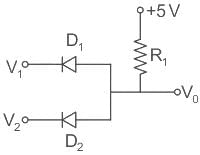
Detailed Solution: Question 17
A signal x(t) = 100 cos (24 π × 103t) is ideally sampled with a sampling period of 50 μsec and then passed through an ideal lowpass filter with a cut-off frequency of 15 kHz. Which of the following frequencies will be present at the filter output:
Detailed Solution: Question 18
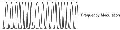
For a given frequency deviation in FM modulation, the modulation index varies______.
Detailed Solution: Question 19
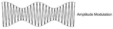
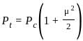
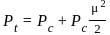
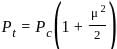
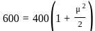
If the total power of an amplitude modulated signal is 600 W and the carrier power is 400 W, the modulation index is
Detailed Solution: Question 20

Refer to the code given below, which kind of circuit is implemented?
PROCESS
BEGIN
WAIT ON X, Y;
Z < = X and Y;
END PROCESS;
PROCESS
BEGIN
WAIT ON X, Y;
Z < = X and Y;
END PROCESS;
Detailed Solution: Question 21
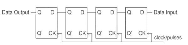
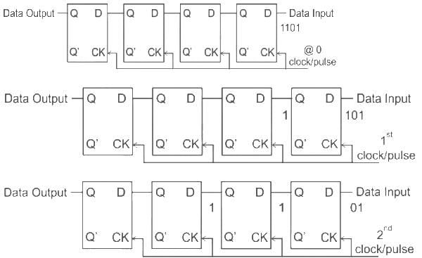
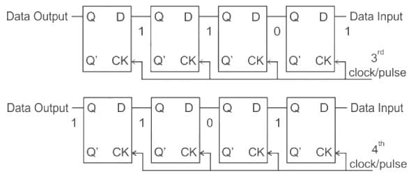
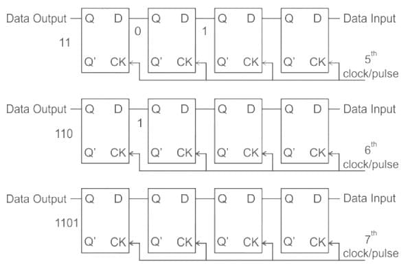
What is the number of clock pulses required to completely load and then unload a 4-bit register?
Detailed Solution: Question 22
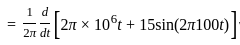
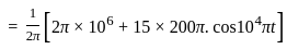
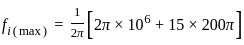
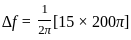
A signal m(t) = 10 cos (2π 100t) is frequency-modulated. The resulting FM signal is x(t) = 20 cos {2π 106 t + 15 sin (2π 100 t)}
The FM bandwidth is nearly
Detailed Solution: Question 23


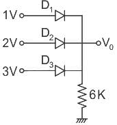
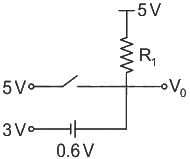
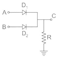
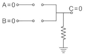
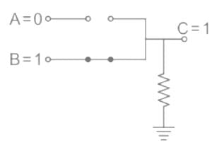
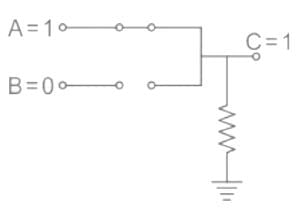
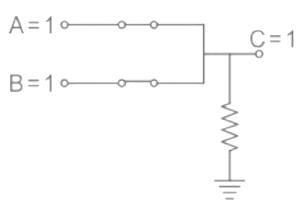
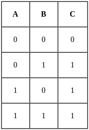
Which of the following logical operations could be computed by the given network?
Detailed Solution: Question 24
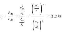
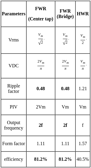
A rectifier (without filter) with fundamental ripple frequency equal to twice the mains frequency, has ripple factor of 0.482 and power conversion efficiency equal to 81.2%. The rectifier is:
i. Bridge rectifier
ii. Full-wave (non bridge) rectifier
iii. Half-wave rectifier.
Which of these are correct?
i. Bridge rectifier
ii. Full-wave (non bridge) rectifier
iii. Half-wave rectifier.
Detailed Solution: Question 25
In root-locus plot, the breakaway points
Detailed Solution: Question 26


Detailed Solution: Question 27
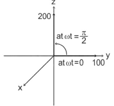
The electric field intensity of the wave is given as
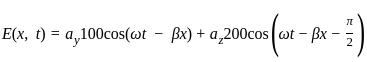
The polarization of the wave is:
The polarization of the wave is:
Detailed Solution: Question 28

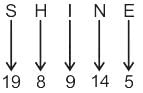
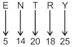
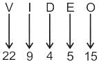
In a certain code language, 'SHINE' is written as '11', and 'ENTRY' is written as '16.4'. How will 'VIDEO' be written in that language?
Detailed Solution: Question 29

Select the number which is different from the others.
Detailed Solution: Question 30