Electrical Engineering (EE) Exam  >  Electrical Engineering (EE) Tests  >  Analog and Digital Electronics  >  Test: Adders - 1 - Electrical Engineering (EE) MCQ

Test: Adders - 1 - Electrical Engineering (EE) MCQ


Test Description

10 Questions MCQ Test Analog and Digital Electronics - Test: Adders - 1

Test: Adders - 1 for Electrical Engineering (EE) 2024 is part of Analog and Digital Electronics preparation. The Test: Adders - 1 questions and answers have been prepared according to the Electrical Engineering (EE) exam syllabus.The Test: Adders - 1 MCQs are made for Electrical Engineering (EE) 2024 Exam. Find important definitions, questions, notes, meanings, examples, exercises, MCQs and online tests for Test: Adders - 1 below.
Solutions of Test: Adders - 1 questions in English are available as part of our Analog and Digital Electronics for Electrical Engineering (EE) & Test: Adders - 1 solutions in Hindi for Analog and Digital Electronics course. Download more important topics, notes, lectures and mock test series for Electrical Engineering (EE) Exam by signing up for free. Attempt Test: Adders - 1 | 10 questions in 30 minutes | Mock test for Electrical Engineering (EE) preparation | Free important questions MCQ to study Analog and Digital Electronics for Electrical Engineering (EE) Exam | Download free PDF with solutions
Test: Adders - 1 - Question 1

Which of the following statements about the arithmetic circuit is INCORRECT?

Detailed Solution for Test: Adders - 1 - Question 1

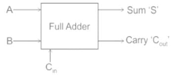
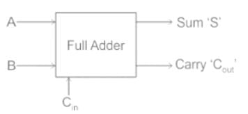
The basic block diagram for a Full Adder is as shown:

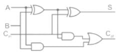
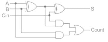
A full adder can be implemented using 2 XOR, 2 AND, 1 OR

Add two bit:

A = A1 A0

B = B1 B0

A0 + B0 will give carry Cin → using half adder 

Now using full adding Add Cin + A1 + B1

Test: Adders - 1 - Question 2

How many number of 2-input NAND gates are required to realise a half adder circuit?

Detailed Solution for Test: Adders - 1 - Question 2

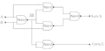
Half Adder using NAND Gates:

The half adder can also be designed with the help of NAND gates. NAND gate is considered as a universal gate. A universal gate can be used for designing any digital circuitry. It is always simple and efficient to use the minimum number of gates in the designing process of our circuit. The minimum number of NAND gates required to design a half adder is 5.

  • The first NAND gate takes the inputs which are the two 1-bit numbers.
  • The resultant NAND-operated inputs will be again given as input to 3- NAND gates along with the original input. 
  • Out of these 3 NAND gates, 2-NAND gates will generate the output which will be given as input to the NAND gate connected at the end.
  • The gate connected at the end will generate the 
1 Crore+ students have signed up on EduRev. Have you? Download the App
Test: Adders - 1 - Question 3

The minimum number of NAND gates requires to implement A ⊕ B ⊕ C is

Detailed Solution for Test: Adders - 1 - Question 3

The Sum output bit of a full adder is given by:

Looking at the Full-Adder circuit, we can see that,

S = A ⊕ B ⊕ C

From full adder circuit,

Cout =  AB + Cin (A ⊕ B)

Now, logic gate for above boolean expression can be drawn as,

Connecting them to a NAND gate, we now have the Full-Adder NAND Equivalent.

Hence, 9 minimum number of NAND gates requires to implement A ⊕ B ⊕ C or Full-Adder circuit.

Test: Adders - 1 - Question 4

A half adder has

Detailed Solution for Test: Adders - 1 - Question 4

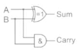
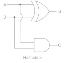
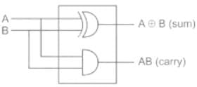
Half adder circuit:

half adder circuit has 2 inputs and 2 outputs.

A half adder circuit is basically made up of an AND gate and an XOR gate as shown below:

Sum (S) = A⊕B

Carry = A.B

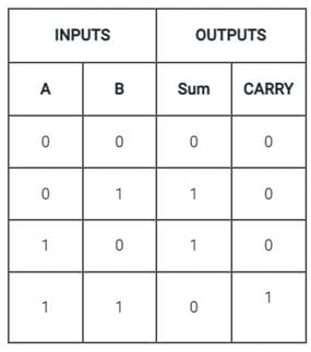
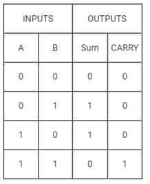
The truth table is as shown:

Important Points:
A full adder circuit has three binary digit inputs (two input bits and one carry input bit) and two binary digit outputs, Sum bit and carry output bit.

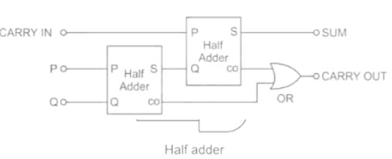
A Full adder can be realized using two half adders as shown:

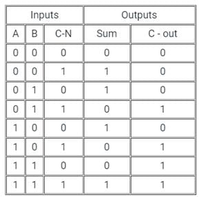
The truth table of a full adder logic is:

The Sum output bit of a full adder is given by:

S = A ⊕ B ⊕ C

The carry output bit of a full adder is given by:

X1 = AB + BC + AC

Test: Adders - 1 - Question 5

The addition of 3-bit is performed using which adder?

Detailed Solution for Test: Adders - 1 - Question 5

Half Adder:  It is a logic circuit that performs addition on two binary digits. It produces a sum and carry.

Full Adder:

  • It is a logic circuit that takes three inputs to perform addition.
  • Two binary input and one carry-in input of the previous stage is used.
  • It generates sum and carry (C-out). C-in is a carry from a less significant digit and c-out is a carry from the most significant bit.


Additional Information
If we want to add two n- bit binary adders then it requires 1 half adder and n-1 full adder to complete the circuit. So, in the given question to add 4- bit binary numbers requires 1 half adder and 3 full adders.

Test: Adders - 1 - Question 6

In case of the parallel adder, the speed with which an addition can be performed is governed by the time required for the carries to propagate or ripple through all the stages of the adder. Which of the following statements are correct?

(A) The method of speeding up the addition process is based on additional functions of full adder called carry generate and carry propagation.

(B) The look-ahead carry adder speeds up the process by eliminating ripple carry dely.

(C) The final sum output of the nth stage is given by Sn = Pn ⊕ Cn where Pn = An ⊕ Bn

(D) The final carry output of nth stage is given by Cn+1 = Gn + Pn where Gn = An ⋅ Bn

Choose the correct answer from the options given below:

(1) (A) and (B) only

(2) (A) and (C) only

(3) (A), (B) and (C) only

(4) (B), (C) and (D) only

Detailed Solution for Test: Adders - 1 - Question 6

Concept:- Carry look-ahead adder

→ In the case of the parallel adder, the speed with which addition can be performed is governed by the time required for the carries to propagate or ripple through all of the stages of the adder.

The look–ahead–carry adder speeds up the process by eliminating this ripple carry delay.

→ It examines all the input bits simultaneously & also generates the carry-in bits for all the stages simultaneously.


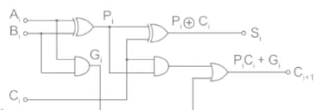
→ Consider the circuit:-
Si = Pi ⊕ Ci

& Pi = Ai ⊕ Bi

Gi = Ai ⋅ Bi

Ci + 1 = Pi Ci + Gi

So, Statements A, B & C are correct only.

Test: Adders - 1 - Question 7

A half adder includes

Detailed Solution for Test: Adders - 1 - Question 7

A half adder circuit is basically made up of an a AND gate with XOR gate as shown below:

  • A half adder is also known as XOR gate because XOR is applied to both inputs to produce the sum
  • Half adder can add only two bits (A and B) and has nothing to do with the carry
  • If the input to a half adder has a carry, then it will neglect it and adds only the A and B bits
  • That means the binary addition process is not complete and that's why it is called a half adder

Sum (S) = A⊕B, Carry = A.B

Test: Adders - 1 - Question 8

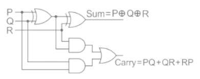
If the inputs are P, Q and R, then in the full adder, find the output expression of the sum.

Detailed Solution for Test: Adders - 1 - Question 8

Full Adder:

Full Adder is the adder that adds three inputs and produces two outputs. The first two inputs are P and Q and the third input R is an input carry.

It is the advantage of full adder over half adder that it can take three inputs together and third input can be an input carry.

Full Adder Circuit:

Full Adder Truth Table:

Test: Adders - 1 - Question 9

Given two half adders, what extra 2-input gate is required to build a full adder?

Detailed Solution for Test: Adders - 1 - Question 9

Half adder:

Full adder:

Full Adder can be implemented using 2 half adders and OR gate as shown below.

Test: Adders - 1 - Question 10

A full adder combinational circuit has

Detailed Solution for Test: Adders - 1 - Question 10

The basic block diagram for a Full Adder is as shown:

A Full adder can be realized using two half adders as shown:


We, therefore, conclude that a full adder combinational circuit has 3 inputs and 2 outputs.

A full adder can be implemented using 2 XOR, 2 AND, 1 OR as shown in figure:

Important Point
The truth table of a full adder logic is:

S = A ⊕ B ⊕ C
The Sum output bit of a full adder is given by:

The carry output bit of a full adder is given by:

X1 = AB + BC + AC

137 videos|143 docs|71 tests
Information about Test: Adders - 1 Page
In this test you can find the Exam questions for Test: Adders - 1 solved & explained in the simplest way possible. Besides giving Questions and answers for Test: Adders - 1, EduRev gives you an ample number of Online tests for practice

Top Courses for Electrical Engineering (EE)

137 videos|143 docs|71 tests
Download as PDF

Top Courses for Electrical Engineering (EE)