Electronics and Communication Engineering (ECE) Exam  >  Electronics and Communication Engineering (ECE) Tests  >  Electronic Devices  >  Test: Common Emitter Configuration - Electronics and Communication Engineering (ECE) MCQ

Test: Common Emitter Configuration - Electronics and Communication Engineering (ECE) MCQ


Test Description

10 Questions MCQ Test Electronic Devices - Test: Common Emitter Configuration

Test: Common Emitter Configuration for Electronics and Communication Engineering (ECE) 2024 is part of Electronic Devices preparation. The Test: Common Emitter Configuration questions and answers have been prepared according to the Electronics and Communication Engineering (ECE) exam syllabus.The Test: Common Emitter Configuration MCQs are made for Electronics and Communication Engineering (ECE) 2024 Exam. Find important definitions, questions, notes, meanings, examples, exercises, MCQs and online tests for Test: Common Emitter Configuration below.
Solutions of Test: Common Emitter Configuration questions in English are available as part of our Electronic Devices for Electronics and Communication Engineering (ECE) & Test: Common Emitter Configuration solutions in Hindi for Electronic Devices course. Download more important topics, notes, lectures and mock test series for Electronics and Communication Engineering (ECE) Exam by signing up for free. Attempt Test: Common Emitter Configuration | 10 questions in 30 minutes | Mock test for Electronics and Communication Engineering (ECE) preparation | Free important questions MCQ to study Electronic Devices for Electronics and Communication Engineering (ECE) Exam | Download free PDF with solutions
Test: Common Emitter Configuration - Question 1

Input resistance of a common emitter transistor of the order of

Detailed Solution for Test: Common Emitter Configuration - Question 1
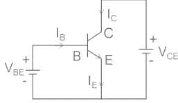
  • In common emitter configuration, the emitter is common to both the base and collector. The emitter-base junction is always forward-biased as the positive terminal of the battery is connected to the p-side of the transistor and the negative terminal of the battery is connected to the n-side of the transistor.
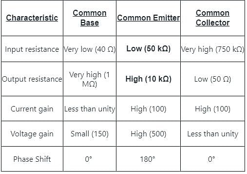
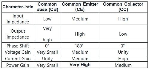
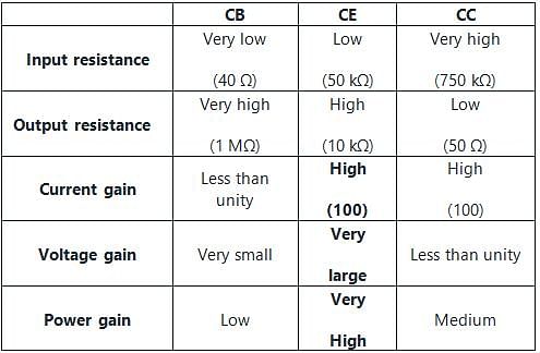
  • The input impedance is typically around 1kΩ, although this can vary considerably according to the circuit values and conditions. The low input impedance results from the fact that the input is applied across the base and emitter where there is a forward-biased junction, Also the output impedance can be relatively high. Again this varies considerably on the electronic component values chosen and current levels permitted. The output impedance may be as high as 10kΩ or possibly more
  • However, if the current drain allows higher current levels to be drawn, the output impedance can be reduced considerably. The level of resistance or impedance comes from the output taken from the collector where there is a reverse-biased junction.

Test: Common Emitter Configuration - Question 2

In a common-emitter amplifier, the input AC signal to be amplified is applied across:

Detailed Solution for Test: Common Emitter Configuration - Question 2

Amplifier: An electronic device that increases the voltage, current, or power of a signal is called an amplifier.

  • Amplifiers are used in wireless communications and broadcasting, and in audio equipment of all kinds.

Common emitter amplifier: It is a three basic single-stage bipolar junction transistor and is used as a voltage amplifier.

  • The input is applied to the base, and the output is taken from the collector, the common terminal for both circuits is the emitter.

The correct option is 1.

1 Crore+ students have signed up on EduRev. Have you? Download the App
Test: Common Emitter Configuration - Question 3

How many degree phases have been shifted from input to output in common emitter configuration? 

Detailed Solution for Test: Common Emitter Configuration - Question 3

Bipolar junction transistor

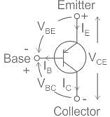
  • The Bipolar Junction Transistor (BJT) is a three-terminal device i.e. Base, Emitter, and Collector.
  • There are two main types of bipolar junction transistors the NPN and the PNP transistor.
  • The emitter is a heavily doped region of the BJT transistor, providing the majority of carriers into the base region.
  • The base region is a thin, lightly doped region sandwiched between the emitter and collector.
  • The majority of carriers from the emitter pass through the base region and its flow can be externally controlled.

Working configuration of BJT

Test: Common Emitter Configuration - Question 4

Which type of configuration has high output impedance but low input impedance? 

Detailed Solution for Test: Common Emitter Configuration - Question 4

Common Base configuration has high output impedance but low input impedance.
Concept:
In common emitter configuration, the emitter terminal is grounded so the common emitter configuration is also known as grounded emitter configuration.

As the emitter current is zero in the cut-off region, the potential VE is called floating emitter potential.

  • The Bipolar Junction Transistor (BJT) is a three-terminal device i.e. Base, Emitter, and Collector.
  • There are two main types of bipolar junction transistors the NPN and the PNP transistor.
  • The emitter is a heavily doped region of the BJT transistor, providing the majority of carriers into the base region.
  • The base region is a thin, lightly doped region sandwiched between the emitter and collector.
  • The majority of carriers from the emitter pass through the base region and its flow can be externally controlled.

Working configuration of BJT

Test: Common Emitter Configuration - Question 5

Which of the following BJT configuration has highest Power Gain?

Detailed Solution for Test: Common Emitter Configuration - Question 5

Test: Common Emitter Configuration - Question 6

In which of the following amplifier configurations, the power gain is the largest? 

Detailed Solution for Test: Common Emitter Configuration - Question 6

Power gain of amplifier:
The power gain of an amplifier is defined as the product of voltage gain and current gain.

where, Ap = Power gain
Av = Voltage gain
Ai = Current gain
Comparison between CE, CC, and CB configuration:

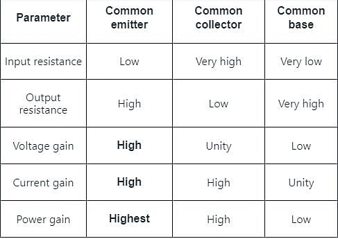
Since the voltage and current gain in the CE amplifier are high, therefore the power gain is maximum.

Test: Common Emitter Configuration - Question 7

In a CE amplifier, collector load is 4 kΩ and quiescent current is 1 mA. Find the operating point if VCC = 10 V.

Detailed Solution for Test: Common Emitter Configuration - Question 7


Given:
VCC = 10V
IC = 1 mA
RC =  4 kΩ
Apply KVL in the collector to Emitter loop:
VCC - ICRC = VC
VC = 10 - 1 mA × 4 kΩ
VC = 10 - 4 = 6V
We know that the operating point is represented in terms of (VC, IC)
Hence the operating point of the given CE Amplifier is 6 V, 1 mA

Test: Common Emitter Configuration - Question 8

For highest power gain, what configuration is used?

Detailed Solution for Test: Common Emitter Configuration - Question 8

Characteristics of Common Emitter Amplifier:
1) The voltage gain and current gain are high
2) The power gain is high
3) There is a phase relationship of 180 degrees in input and output
4) The input and output resistors are medium

Test: Common Emitter Configuration - Question 9

The most widely used amplifier configuration is

Detailed Solution for Test: Common Emitter Configuration - Question 9

Common emitter configuration:

  • The emitter is connected between the collector and base.
  • The emitter is common to both the input and the output circuit.
  • Both current and voltage gain can be described as medium.
  • This provides good overall performance and as such, it is often the most widely used configuration.
Test: Common Emitter Configuration - Question 10

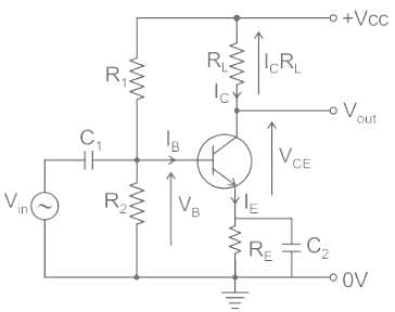
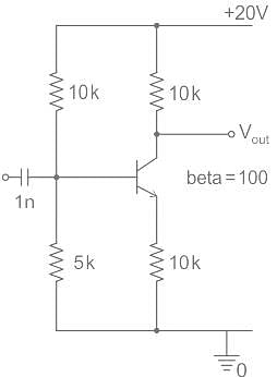
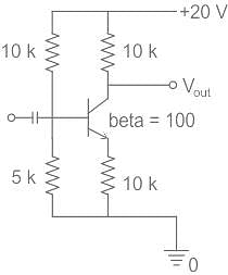
Given figure shows a silicon transistor connected as a common emitter amplifier. The quiescent collector voltage of the circuit is approximately.
Detailed Solution for Test: Common Emitter Configuration - Question 10

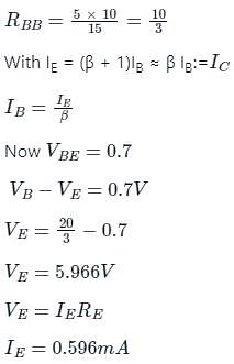
The quiescent Base voltage (Vb) is determined by the potential divider network formed by the two resistors R1, R(connected to the base of the transistor), and the power supply voltage Vcc as shown, with the current flowing through both the resistors.


The Thevenin equivalent resistance connected to the base of the circuit will be:

Assuming IE ≈ IC, the output voltage will be:

21 docs|29 tests
Information about Test: Common Emitter Configuration Page
In this test you can find the Exam questions for Test: Common Emitter Configuration solved & explained in the simplest way possible. Besides giving Questions and answers for Test: Common Emitter Configuration, EduRev gives you an ample number of Online tests for practice

Top Courses for Electronics and Communication Engineering (ECE)

Download as PDF

Top Courses for Electronics and Communication Engineering (ECE)