Test: Differential Amplifiers - Electronics and Communication Engineering (ECE) MCQ
10 Questions MCQ Test Topicwise Question Bank for Electronics Engineering - Test: Differential Amplifiers
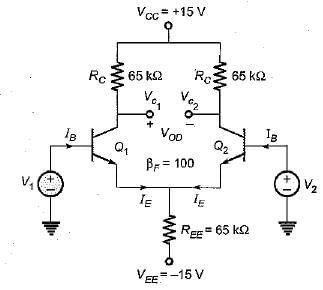
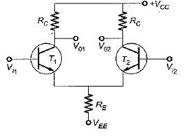
A resitive loaded and biased differential amplifier circuit is shown in figure. Neglecting the base currents and assuming matched transistors with VA = ∞,β = 100, w hat are the values of Rc and RE to meet the following specifications?
Differential mode gain (double ended) = -500,
Common mode rejection ratio = 500,
Differential mode input resistance = 2 MQ.

Differential mode gain (double ended) = -500,
Common mode rejection ratio = 500,
Differential mode input resistance = 2 MQ.


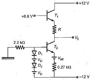
In the level shifter circuit shown in figure beiow, the internal drop across each diode VD = VBE2 = 0.7 V and hfe is very large.
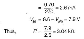
The value of R for V0 to become zero is

The value of R for V0 to become zero is

| 1 Crore+ students have signed up on EduRev. Have you? Download the App |
Most of linear ICs are based on the two transistor differential amplifier because of its
A CE amplifier has RL = 10 KΩ. Given that hie = 1 KΩ, hfe = 50, hre = 0 and 1/hoe = 40 KΩ. Calculate the voltage gain.
In a single-stage differential amplifier, the output offset voltage is basically dependent on the mismatch of
Assertion (A): It is not so easy to design d.c. amplifiers using transistors.
Reason (R): The values of hfe ,VBE and ICBO vary with temperature.
Assertion (A): The ability of a differential amplifier to reject a differential mode signal is called its “figure of merit”.
Reason (R): The ideal value of figure of merit of a differential amplifier is infinite.
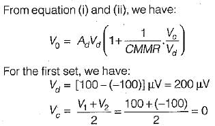
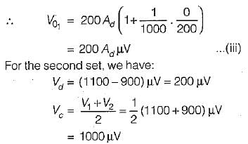
A differential amplifier has (i) CMMR= 1000 and (ii) CMRR= 10000.
The first set of inputs is V1= 100 μV and V2, = -100μV.
The second set of inputs is V1= 1100 μV and V2 = 900 μV.
What is the percentage difference in output voltage obtained for the two sets of input voltages?
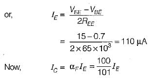
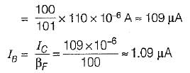
The Q-point (Vc and IB) for the differential amplifier shown in figure below is given by:
