GATE Electrical Engineering (EE) Test: Diode Circuits - 2 Free Online Test
MCQ Practice Test & Solutions: Test: Diode Circuits - 2 (15 Questions)
You can prepare effectively for Electrical Engineering (EE) GATE Electrical Engineering (EE) Mock Test Series 2027 with this dedicated MCQ Practice Test (available with solutions) on the important topic of "Test: Diode Circuits - 2". These 15 questions have been designed by the experts with the latest curriculum of Electrical Engineering (EE) 2026, to help you master the concept.
Test Highlights:
- - Format: Multiple Choice Questions (MCQ)
- - Duration: 45 minutes
- - Number of Questions: 15
Sign up on EduRev for free to attempt this test and track your preparation progress.

In the question a circuit and a waveform for the input voltage is given. The diode in circuit has cutin voltage Vγ = 0. Choose the option for the waveform of output voltage vo :
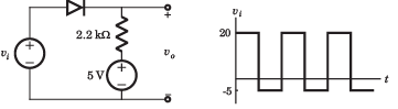
Detailed Solution: Question 1
In the question a circuit and a waveform for the input voltage is given. The diode in circuit has cutin voltage Vγ = 0. Choose the option for the waveform of output voltage vo:
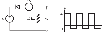
Detailed Solution: Question 2

In the question a circuit and a waveform for the input voltage is given. The diode in circuit has cutin voltage Vγ = 0. Choose the option for the waveform of output voltage vo
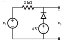
Detailed Solution: Question 3
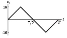
In the question a circuit and a waveform for the input voltage is given. The diode in circuit has cutin voltage Vγ = 0. Choose the option for the waveform of output voltage vo
Detailed Solution: Question 4
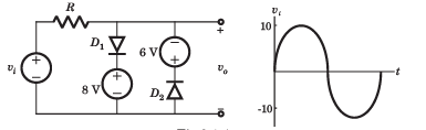
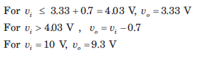
For the circuit in fig. P.3.1.5, let cutin voltage Vγ = 0.7 V. The plot of vo verses vi for -10 ≤ vi ≤10 V is:
Detailed Solution: Question 5
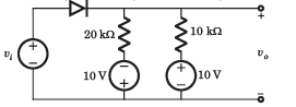
The circuit inside the box in fig. contains only resistor and diodes. The terminal voltage vo is connected to some point in the circuit inside the box. The largest and smallest possible value of vo most nearly to is respectively.
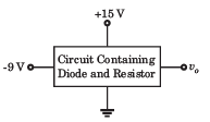
Detailed Solution: Question 6
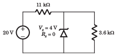
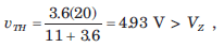
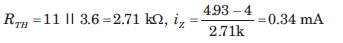
In the voltage regulator circuit in fig. the maximum load current iL that can be drawn is:
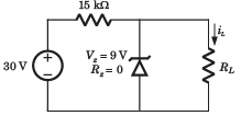
Detailed Solution: Question 7
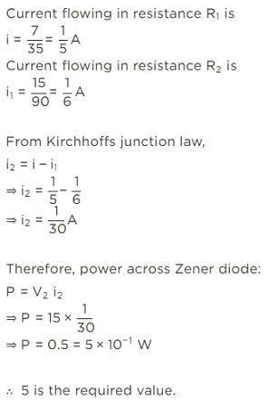
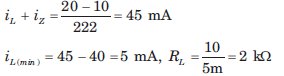
The value of power dissipated across the Zener diode (Vz=15 V) connected in the circuit as shown in the figure is x × 10−1 watts.
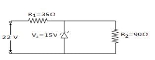
The value of x to the nearest integer is
The value of x to the nearest integer is
Detailed Solution: Question 8

Detailed Solution: Question 9
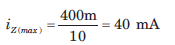
In the voltage regulator circuit in fig the power rating of Zener diode is 400 mW. The value of RL that will establish maximum power in Zener diode is:
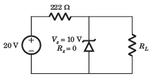
Detailed Solution: Question 10
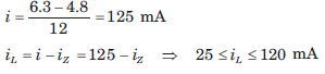
In the voltage regulator circuit in fig. the Zener diode current is to be limited to the range 5 ≤ iz ≤100 mA.
The range of possible load current is:
Detailed Solution: Question 11
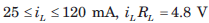
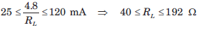
In the voltage regulator circuit in fig. the Zener diode current is to be limited to the range 5 ≤ iz ≤100 mA.
The range of possible load resistance is:
Detailed Solution: Question 12
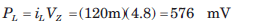
In the voltage regulator circuit in fig. the Zener diode current is to be limited to the range 5 ≤ iz ≤100 mA.
The power rating required for the load resistor is:
Detailed Solution: Question 13
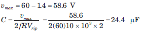
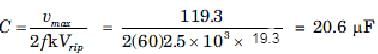
The secondary transformer voltage of the rectifier circuit shown in fig. is vs = 60 sin 2π 60tV. Each diode has a cut in voltage of Vγ = 0.6 V. The ripple voltage is to be no more than Vrip = 2 V. The value of filter capacitor will be:
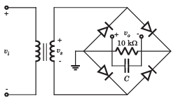
Detailed Solution: Question 14
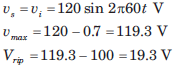
The input to full-wave rectifier in fig. is vi = 120 sin2π60t V. The diode cutin voltage is 0.7 V. If the output voltage cannot drop below 100 V, the required value of the capacitor is:
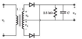
Detailed Solution: Question 15
26 docs|247 tests |