Electronics and Communication Engineering (ECE) Exam  >  Electronics and Communication Engineering (ECE) Tests  >  GATE ECE (Electronics) Mock Test Series 2025  >  Test: Electronic Devices - 2 - Electronics and Communication Engineering (ECE) MCQ

Test: Electronic Devices - 2 - Electronics and Communication Engineering (ECE) MCQ


Test Description

20 Questions MCQ Test GATE ECE (Electronics) Mock Test Series 2025 - Test: Electronic Devices - 2

Test: Electronic Devices - 2 for Electronics and Communication Engineering (ECE) 2024 is part of GATE ECE (Electronics) Mock Test Series 2025 preparation. The Test: Electronic Devices - 2 questions and answers have been prepared according to the Electronics and Communication Engineering (ECE) exam syllabus.The Test: Electronic Devices - 2 MCQs are made for Electronics and Communication Engineering (ECE) 2024 Exam. Find important definitions, questions, notes, meanings, examples, exercises, MCQs and online tests for Test: Electronic Devices - 2 below.
Solutions of Test: Electronic Devices - 2 questions in English are available as part of our GATE ECE (Electronics) Mock Test Series 2025 for Electronics and Communication Engineering (ECE) & Test: Electronic Devices - 2 solutions in Hindi for GATE ECE (Electronics) Mock Test Series 2025 course. Download more important topics, notes, lectures and mock test series for Electronics and Communication Engineering (ECE) Exam by signing up for free. Attempt Test: Electronic Devices - 2 | 20 questions in 60 minutes | Mock test for Electronics and Communication Engineering (ECE) preparation | Free important questions MCQ to study GATE ECE (Electronics) Mock Test Series 2025 for Electronics and Communication Engineering (ECE) Exam | Download free PDF with solutions
Test: Electronic Devices - 2 - Question 1

For a MOS capacitor, Vfb and Vare the flat-band voltage and the threshold voltage, respectively. The variation of the depletion width (Wdep) for varying gate voltage (Vg) is best represented by

Detailed Solution for Test: Electronic Devices - 2 - Question 1

1. Key Concepts:

  • Flat-band voltage (VfbV_{fb}): The gate voltage at which there is no band bending in the semiconductor, and the depletion region width is zero (Wdep=0W_{\text{dep}} = 0).
  • Threshold voltage (VtV_t): The gate voltage at which the inversion layer forms, and the depletion region width reaches its maximum.
  • Depletion width (WdepW_{\text{dep}}): The width of the region in the semiconductor where mobile carriers are depleted under the influence of an electric field.

2. Depletion Width Regions:

  • Region 1: Vg<VfbV_g < V_{fb}: In this region, the gate voltage is insufficient to bend the bands, and the depletion region does not form:

    Wdep=0W_{\text{dep}} = 0
  • Region 2: Vfb<Vg<VtV_{fb} < V_g < V_t: In this region, as VgV_g increases, a depletion region begins to form, and its width increases with the gate voltage. The depletion width is given by:

    Wdep=2ϵsqNd(VgVfb)W_{\text{dep}} = \sqrt{\frac{2 \epsilon_s}{q N_d} (V_g - V_{fb})}

    Where:

    • ϵs\epsilon_s: Permittivity of the semiconductor,
    • qq: Charge of an electron (1.6×10¹⁹C1.6 \times 10^{-19} \, C),
    • NdN_d: Doping concentration of the semiconductor.
  • Region 3: Vg>VtV_g > V_t: Once the gate voltage exceeds the threshold voltage, the depletion width saturates and becomes constant. This is because any further increase in VgV_g causes the formation of an inversion layer, preventing further expansion of the depletion region:

    Wdep=Wdep, maxW_{\text{dep}} = W_{\text{dep, max}}

    Wdep, maxW_{\text{dep, max}} is determined by:

    Wdep, max=2ϵsqNd(VtVfb)W_{\text{dep, max}} = \sqrt{\frac{2 \epsilon_s}{q N_d} (V_t - V_{fb})}

3. Example Substitution:

Let’s assume typical values:

  • ϵs=1.05×10¹²F/m\epsilon_s = 1.05 \times 10^{-12} \, F/m (for silicon),
  • q=1.6×10¹⁹Cq = 1.6 \times 10^{-19} \, C,
  • Nd=1016cm3=1022m3N_d = 10^{16} \, \text{cm}^{-3} = 10^{22} \, \text{m}^{-3},
  • Vfb=1VV_{fb} = -1 \, V,
  • Vt=1VV_t = 1 \, V,
  • Vg=0.5VV_g = 0.5 \, V (in the depletion region).

Calculation:

  1. For Vfb<Vg<VtV_{fb} < V_g < V_t (Vg=0.5VV_g = 0.5 \, V):

    Wdep=2(1.05×10¹²)(1.6×10¹⁹)(1022)(0.5(1))W_{\text{dep}} = \sqrt{\frac{2 (1.05 \times 10^{-12})}{(1.6 \times 10^{-19}) (10^{22})} (0.5 - (-1))}

    Simplifying:

    Wdep=2.1×10121.6×1031.5W_{\text{dep}} = \sqrt{\frac{2.1 \times 10^{-12}}{1.6 \times 10^{3}} \cdot 1.5} Wdep=1.96875×10¹⁵W_{\text{dep}} = \sqrt{1.96875 \times 10^{-15}} Wdep1.4×108m=14nmW_{\text{dep}} \approx 1.4 \times 10^{-8} \, \text{m} = 14 \, \text{nm}
  2. For Vg>VtV_g > V_t (Vg=2VV_g = 2 \, V):

    Wdep=Wdep, max=2(1.05×10¹²)(1.6×10¹⁹)(1022)(1(1))W_{\text{dep}} = W_{\text{dep, max}} = \sqrt{\frac{2 (1.05 \times 10^{-12})}{(1.6 \times 10^{-19}) (10^{22})} (1 - (-1))}

    Simplifying:

    Wdep, max=2.1×10121.6×1032W_{\text{dep, max}} = \sqrt{\frac{2.1 \times 10^{-12}}{1.6 \times 10^{3}} \cdot 2} Wdep, max=2.625×10¹⁵W_{\text{dep, max}} = \sqrt{2.625 \times 10^{-15}} Wdep, max1.62×108m=16.2nmW_{\text{dep, max}} \approx 1.62 \times 10^{-8} \, \text{m} = 16.2 \, \text{nm}

4. Interpretation of Results:

  • When Vg<VfbV_g < V_{fb}: Wdep=0W_{\text{dep}} = 0,
  • When Vfb<Vg<VtV_{fb} < V_g < V_t: Wdep=14nmW_{\text{dep}} = 14 \, \text{nm} (increases with VgV_g),
  • When Vg>VtV_g > V_t: Wdep=16.2nmW_{\text{dep}} = 16.2 \, \text{nm} (saturates).
Test: Electronic Devices - 2 - Question 2

Two n-channel MOSFETs, T1 and T2, are identical in all respects except that the width of T2 is double of T1. Both the transistor are biased in the saturation region of operation, but the gate overdrive voltage (VGS - VTH) of T2 is double that of T1, where VGS and VTH are the gate-to-source voltage and threshold voltage of the transistors, respectively. If the drain current and transconductance of T1 are ID1 and gm1 respectively ; the corresponding values of these two parameters for T2 are

Detailed Solution for Test: Electronic Devices - 2 - Question 2

Given, two transistors T1 and T2 which are identical in all respects except for width and gate overdrive voltage (VGS - Vth).
For T1 MOSFET,

gm1 ∝ W(VGS - Vth)1  and  ID1 ∝ W1 (VGS - Vth)21

Similarly for T2, gm2 ∝ W2 (VGS - Vth)2  and  ID2 ∝ W2 (VGS - Vth)22

Given W2 = 2W1,

And (VGS - V­th)2 = 2 (VGS - Vth)1

Putting these in Equation (1), we get,

Similarly,

gm2 = 4gm

1 Crore+ students have signed up on EduRev. Have you? Download the App
Test: Electronic Devices - 2 - Question 3

If saturation currents of 2 diodes are 1 µA and 2 µA.
If break down voltages of diode are same and are equal to 100 volt, what is value of current in D1.
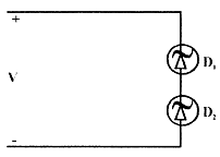
Q.

If V = 90 volt

Test: Electronic Devices - 2 - Question 4

If saturation currents of 2 diodes are 1 µA and 2 µA.
If break down voltages of diode are same and are equal to 100 volt, what is value of current in D1.

Q.

If V = 110 volt

Test: Electronic Devices - 2 - Question 5

For Si transistor, if β ≥ 30 and ICBO = 10 nA  The minimum value of R, for transistor to remain in active region for vi = 12 volt, is __________ kΩ.

Test: Electronic Devices - 2 - Question 6

A sample of silicon (uniformly doped n-type) at T = 300° K has the electron concentration varying linearly with distance as shown in the figure

The diffusion current is found to be −1120 A/cm2. If the diffusion constant Dn = 35 cm2/s, the electron concentration at x = 0 is

Detailed Solution for Test: Electronic Devices - 2 - Question 6

Test: Electronic Devices - 2 - Question 7

In a semiconductor sample,

where LP (hole diffusion length) = 4.8 × 10⁻⁴ cm

Hole diffusion coefficient DP = 20 cm2/s

The hole diffusion current density at x = 0 is

Detailed Solution for Test: Electronic Devices - 2 - Question 7

Test: Electronic Devices - 2 - Question 8

In the plot of log I vs V for a semiconductor Ge diode, the slope at room temperature is _________. Assume V >> VT and room temperature 27°C.

Detailed Solution for Test: Electronic Devices - 2 - Question 8

Test: Electronic Devices - 2 - Question 9

Consider a p-type semiconductor which is lightly doped i.e. condition of p >> n is not valid. p, n, ni are holes, electrons and intrinsic carrier concentration respectively. Then 2n + NA is ___________ if NA is immobile acceptor ions concentration

Detailed Solution for Test: Electronic Devices - 2 - Question 9

According to charge neutrality,

Test: Electronic Devices - 2 - Question 10

Consider the following network 

VL is to be maintained at 10 V.
The correct representation of VL versus RL is

Detailed Solution for Test: Electronic Devices - 2 - Question 10

RLmin to turn-on the zener diode 

Test: Electronic Devices - 2 - Question 11

Consider the following sentences in respect of LEDs (Light emitting diodes) and semiconductor laser diode.
S1 :  Only direct band gap type semiconductors are suitable for fabrication of LEDs.
S2 : Both direct band gap type and indirect band gap type semiconductors are suitable for fabrication of semiconductor laser diode.
Choose the best alternative

Detailed Solution for Test: Electronic Devices - 2 - Question 11

For the fabrication of semiconductor laser diode, direct band gap type semiconductor is required

Test: Electronic Devices - 2 - Question 12

An n-channel enhancement mode MOSFET is biased at VGS > VTH and VDS > (VGS - VTH), where VGS is the gate-to-source voltage, VDS is the drain-to-source voltage and VTH is the threshold voltage. Considering channel length modulation effect to be significant, the MOSFET behaves as a

Detailed Solution for Test: Electronic Devices - 2 - Question 12

- In the given condition VGS > VTH and VDS > (VGS - VTH), the MOSFET operates in the saturation region.
- In the saturation region, the MOSFET behaves as a current source.
- Channel length modulation affects the output characteristics, making the output impedance finite rather than infinite, as the drain current \(ID) depends on ( VDS).
- Therefore, the MOSFET acts as a current source with finite output impedance, which corresponds to option C.

Test: Electronic Devices - 2 - Question 13

What are the states of three ideal diodes of circuit shown below:

Test: Electronic Devices - 2 - Question 14

For BJT, circuit shown assume that β of transistor is very large, if here Si transistor is used, then transistor will operate in

Detailed Solution for Test: Electronic Devices - 2 - Question 14

If β is large then transistor will be in S.R

Test: Electronic Devices - 2 - Question 15

Consider the following circuit:

Q.

If vi is as shown

then RB and RC for the circuit concerned can be _________ and _________ respectively, if ICsat = 6 mA. Assume the transistor inverter operation

Detailed Solution for Test: Electronic Devices - 2 - Question 15

Just at onset of saturation,


Test: Electronic Devices - 2 - Question 16

Consider the following circuit:

Q.

The V0 shall be represented by

Detailed Solution for Test: Electronic Devices - 2 - Question 16

Transistor is switch in inverter operation.

Test: Electronic Devices - 2 - Question 17

A BJT having β = 125 is biased at a dc collector current of 1.23 mA. The values of gm, re and rπ at the bias point are: (Assume temperature of operation = 25°C).

Detailed Solution for Test: Electronic Devices - 2 - Question 17

Test: Electronic Devices - 2 - Question 18

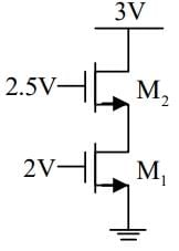
Assuming that transistor M1 and M2 are identical and have a threshold voltage of 1V, the state of transistors M1 and M2 are respectively

Detailed Solution for Test: Electronic Devices - 2 - Question 18

For the given figure,

Let x be the voltage at node A.

Now, VDS2 = 3 − x

VGS2 − Vt = 2.5 − x − 1

= 1.5 - x

We observe that, VDS2 is always > VGS2 − Vt

So, M2 will always be in saturation.

Assuming M1 to be in saturation, we calculate the saturation current as shown.

(IDSat)1 = (IDSat)2

⇒ Kn(VGS - Vt)21 = Kn (VGS - Vt)22

⇒ (2 - 1)2 = (2.5 - x - 1)2

⇒ 1 = 1.5 - x

x = 0.5 V

If ‘x’ were to be 0.5 V then for M1,

VDS = x - 0 = 0.5 V

and VGS - V= 1 V

So, VDS < VGS - Vt

This shows that our assumption is wrong, and M1 cannot be in saturation.

So, M1 is in cut off.

Test: Electronic Devices - 2 - Question 19

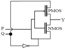
For the circuit shown in the figure, P and Q are the inputs and Y is the output.

The logic implemented by the circuit is

Detailed Solution for Test: Electronic Devices - 2 - Question 19

⇒ If P = high:

PMOS is OFF

NMOS is ON 

then y = Q̅

⇒If P = low

PMOS is ON

NMOS is OFF 

then  y = Q

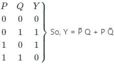
The truth table of the above will be as shown:

= P ⊕ Q

So, Ex – OR Operation is being performed. 

Test: Electronic Devices - 2 - Question 20

The figure shows the band diagram of a Metal Oxide Semiconductor (MOS). The surface region of this MOS is in
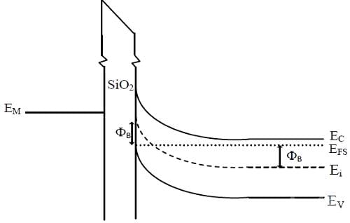
Detailed Solution for Test: Electronic Devices - 2 - Question 20

When the semiconductor in a MOS is in inversion, the intrinsic energy level crosses over Fermi level and goes as deep into the other side of Fermi at the interface as distant it is from the Fermi level in the bulk.

Here, the intrinsic Femi level is below EFS by ϕin the bulk and above EFS by ϕat the interface. Thus the MOS is in inversion.

25 docs|263 tests
Information about Test: Electronic Devices - 2 Page
In this test you can find the Exam questions for Test: Electronic Devices - 2 solved & explained in the simplest way possible. Besides giving Questions and answers for Test: Electronic Devices - 2, EduRev gives you an ample number of Online tests for practice

Top Courses for Electronics and Communication Engineering (ECE)

Download as PDF

Top Courses for Electronics and Communication Engineering (ECE)