Test: MOSFET - 2 - Electronics and Communication Engineering (ECE) MCQ


Test Description

10 Questions MCQ Test GATE ECE (Electronics) Mock Test Series 2025 - Test: MOSFET - 2

Test: MOSFET - 2 for Electronics and Communication Engineering (ECE) 2024 is part of GATE ECE (Electronics) Mock Test Series 2025 preparation. The Test: MOSFET - 2 questions and answers have been prepared according to the Electronics and Communication Engineering (ECE) exam syllabus.The Test: MOSFET - 2 MCQs are made for Electronics and Communication Engineering (ECE) 2024 Exam. Find important definitions, questions, notes, meanings, examples, exercises, MCQs and online tests for Test: MOSFET - 2 below.
Solutions of Test: MOSFET - 2 questions in English are available as part of our GATE ECE (Electronics) Mock Test Series 2025 for Electronics and Communication Engineering (ECE) & Test: MOSFET - 2 solutions in Hindi for GATE ECE (Electronics) Mock Test Series 2025 course. Download more important topics, notes, lectures and mock test series for Electronics and Communication Engineering (ECE) Exam by signing up for free. Attempt Test: MOSFET - 2 | 10 questions in 30 minutes | Mock test for Electronics and Communication Engineering (ECE) preparation | Free important questions MCQ to study GATE ECE (Electronics) Mock Test Series 2025 for Electronics and Communication Engineering (ECE) Exam | Download free PDF with solutions
Test: MOSFET - 2 - Question 1

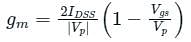
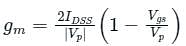
An N-channel JFET has IDSS = 1 mA and VP = -8V. Its maximum transconductance is ________

Detailed Solution for Test: MOSFET - 2 - Question 1

The drain current in saturation for a JFET is given by:

IDSS = Saturation Drain Current
Vp = Pinch Off Voltage
The transconductance (gm) is defined as the change in ID with respect to a change in the gate to source voltage (VGS), i.e.

Taking the differentiation of Equation (1), we get:

The maximum value of gm occurs when VGS = 0

Calculation:
Given:
IDSS = 1 mA, Vp = -8V
We can write:
Maximum transconductance


Test: MOSFET - 2 - Question 2

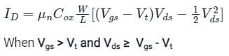
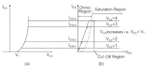
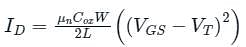
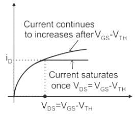
The (Id - Vgs) characteristics of a MOSFET in the saturation region is:

Detailed Solution for Test: MOSFET - 2 - Question 2

The current equations for the MOSFET in different regions are shown below:
When the Vgs < Vt
NMOS operates in the cutoff region and current ID = 0
When Vgs > Vt and Vds < Vgs - Vt 
NMOS operates in the linear region
The current is defined as:

NMOS operates in the saturation region
The current is defined as:

Hence, we can see that in the saturation region the relation between Id and Vgs is quadratic.
Analysis:

1 Crore+ students have signed up on EduRev. Have you? Download the App
Test: MOSFET - 2 - Question 3

For n-channel depletion JFET, the highest trans-conductance gain for a small signal is at

Detailed Solution for Test: MOSFET - 2 - Question 3

The current equation for a depletion type JFET is given by:

IDSS = Saturation Current of the JFET
VGS = Gate to source voltage applied
VP = Pinch off voltage at which ID = IDSS, which is also the voltage at which the channel ceases to exist. It is also denoted by VGS(off).
The transconductance (gm) is defined as the change in ID with respect to a change in the gate to source voltage (VGS), i.e.

Taking the differentiation of Equation (1), we get:

The maximum value of gm occurs when Vgs = 0

gm0 is the maximum transconductance at VGS = 0

The characteristic graph for a change in VGS is as shown:

Test: MOSFET - 2 - Question 4

The drain current in MOSFET is varied by:

Detailed Solution for Test: MOSFET - 2 - Question 4

The drain current in MOSFET in saturation is given by:

Observation:
From the equation, we can observe that the MOSFET’s drain current depends on:
1) Device parameters W/L
2) Gate to Source Voltage VGS
To realize this physically, as the Gate to source voltage is increased, the channel becomes deeper, hence there is more area through which electrons can move.

Test: MOSFET - 2 - Question 5

In which of the following cases, MOSFET is helpful?
(I) Switch for LED
(II) Switch with hysteresis
(III) Switching Solenoid

Detailed Solution for Test: MOSFET - 2 - Question 5

MOSFET (Metal Oxide Semiconductor Field Effect Transistor):
MOSFET transistor is a semiconductor device that is used for amplifying and switching electronic signals in electronic devices.

MOSFET is of two types:
1. Enhancement MOSFET:

  • In this kind of MOSFET, there is no predefined channel. The channel is constructed using the gate to source applied voltage.
  • The more is the voltage on the gate, the better the device can conduct.

2. Depletion mode MOSFET:

  • In this type of MOSFET, the channel (between drain and source) is predefined and the MOSFET conducts without any application of the gate voltage.
  • As the voltage on the gate is either positive or negative,  the channel conductivity decreases.
  • Depletion MOSFET can work in both depletion and enhancement mode.

MOSFET can be used in multiple ways such as:

  • MOSFET as a switch for LED.
  • MOSFET as a switch for Arduino.
  • MOSFET switch for ac load.
  • MOSFET switch for dc motor.
  • MOSFET switch for negative voltage.
  • MOSFET as a switch with a microcontroller.
  • MOSFET switch with hysteresis.
  • MOSFET as switch diode and active resistor.
  • MOSFET as a switch equation.
  • MOSFET switch for airsoft.
  • MOSFET as switch gate resistor.
  • MOSFET as a switching solenoid.
  • MOSFET switch using an optocoupler.
Test: MOSFET - 2 - Question 6

The effective channel length of MOSFET in saturation decreases with increase in

Detailed Solution for Test: MOSFET - 2 - Question 6
  • Ideal enhancement MOSFET is a MOSFET which saturates when VDS ≥ VGS - VT and allows a constant current to flow across it even after a further increase in VDS.
  • But for a non-ideal MOSFET (i.e. MOSFET in which channel length modulation effect is significant), a change in VDS beyond VGS - VT, will result in a further increase in current beyond saturation. This effect is known as channel length modulation.
  • This is explained with the help of the following diagram:


Also, the output characteristics will be as shown:

now is no longer infinite.

Test: MOSFET - 2 - Question 7

A CMOS amplifier when compared to an N–channel MOSFET, has the advantage of

Detailed Solution for Test: MOSFET - 2 - Question 7

Complementary Metal-oxide-semiconductor (CMOS) uses complementary & symmetrical pair of P-type & n-type MOSFETS.

  • The two important characteristics of CMOS devices are high noise immunity and low power dissipation.
  • CMOS devices dissipate less power than NMOS devices because the CMOS dissipates power only when switching (“dynamic power), whereas N channel MOSFET dissipates power whenever the transistor is on because there is a current path from Vdd to Vss.
  • In a CMOS, only one MOSFET is switched on at a time. Thus, there is no path from voltage source to ground so that a current can flow. Current flows in a MOSFET only during switching.
  • Thus, compared to N-channel MOSFET has the advantage of lower drain current from the power supply, thereby causing less power dissipation.
Test: MOSFET - 2 - Question 8

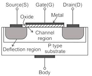
The O in a MOSFET stands for _______ layer which provides _______ to the device.

Detailed Solution for Test: MOSFET - 2 - Question 8

The O in a MOSFET stands for Oxide layer which provides high input impedance to the device.

MOSFET:
A Metal Oxide Semiconductor Field Effect Transistor (MOSFET) has 4 terminals Gate, Drain, Source, and Substrate (Body) terminal. But in many practical circuits MOSFET is used by connecting three terminals Gate, Drain, and Source while connecting the Substrate (Body) terminal to the source.


drain, source, the gate is the terminal for MOSFET.

Test: MOSFET - 2 - Question 9

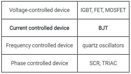
Which of the following power electronics devices can carry DC current in both directions?

Detailed Solution for Test: MOSFET - 2 - Question 9

MOSFET:

  • MOSFET can carry DC current in both directions.
  • The MOSFET channel itself can conduct current in either direction.
  • And in addition, it has this built-in body diode that can conduct a negative current.
  • Due to the itegral body diode, most discrete MOSFETs cannot block in the reverse direction, but the channel will conduct in either direction when the gate is biased "ON".
  • So the MOSFET by itself can be a current bidirectional two-quadrant switch.

  • The body diode of practical MOSFETs may not be a very good diode.
  • So if we have a slow body diode we might not want to let it conduct and have to switch it off because of its slow switching time.
  • Thus we have to put an external diode in series with a MOSFET that only lets the current flow in the positive direction.
  • And then put in externally an antiparallel diode to get a current bidirectional switch.
Test: MOSFET - 2 - Question 10

Power MOSFETs (MOSFETs) are classified as which type of power electronics device?

Detailed Solution for Test: MOSFET - 2 - Question 10

25 docs|263 tests
Information about Test: MOSFET - 2 Page
In this test you can find the Exam questions for Test: MOSFET - 2 solved & explained in the simplest way possible. Besides giving Questions and answers for Test: MOSFET - 2, EduRev gives you an ample number of Online tests for practice

Top Courses for Electronics and Communication Engineering (ECE)

Download as PDF

Top Courses for Electronics and Communication Engineering (ECE)