Electrical Engineering (EE) Exam  >  Electrical Engineering (EE) Tests  >  Digital Electronics  >  Test: Shift Registers - 2 - Electrical Engineering (EE) MCQ

Test: Shift Registers - 2 - Electrical Engineering (EE) MCQ


Test Description

10 Questions MCQ Test Digital Electronics - Test: Shift Registers - 2

Test: Shift Registers - 2 for Electrical Engineering (EE) 2024 is part of Digital Electronics preparation. The Test: Shift Registers - 2 questions and answers have been prepared according to the Electrical Engineering (EE) exam syllabus.The Test: Shift Registers - 2 MCQs are made for Electrical Engineering (EE) 2024 Exam. Find important definitions, questions, notes, meanings, examples, exercises, MCQs and online tests for Test: Shift Registers - 2 below.
Solutions of Test: Shift Registers - 2 questions in English are available as part of our Digital Electronics for Electrical Engineering (EE) & Test: Shift Registers - 2 solutions in Hindi for Digital Electronics course. Download more important topics, notes, lectures and mock test series for Electrical Engineering (EE) Exam by signing up for free. Attempt Test: Shift Registers - 2 | 10 questions in 20 minutes | Mock test for Electrical Engineering (EE) preparation | Free important questions MCQ to study Digital Electronics for Electrical Engineering (EE) Exam | Download free PDF with solutions
Test: Shift Registers - 2 - Question 1

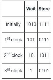
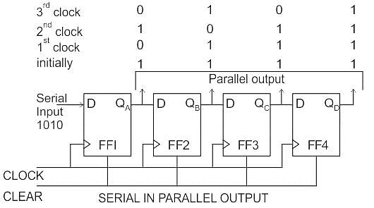
A 4 bit serial in parallel out shift register is initially set to 1111. The data 1010 is applied to the input. After 3 clock cycles the output will be:

Detailed Solution for Test: Shift Registers - 2 - Question 1

Concept: In serial IN/Parallel out shift register data will be shifted all at a time with every clock pulse.

since initially 1111 stored

so after 3rd clock pulse output will be 0101

Test: Shift Registers - 2 - Question 2

Observe the below code and choose the correct option.

architecture behave of ckt is

signal temp: std_logic vector (7 downto 0);

begin

process(clock)

begin

if (clock’event and clock=’1’) then

for i in 0 to 6 loop

temp(i + 1) <= temp(i);

end loop;

temp(0) <= sin;

end if;

end process;

sout <= temp(7);

end behave;

Detailed Solution for Test: Shift Registers - 2 - Question 2

This is represented when the process has the clock signal in its sensitivity list else we can’t call that a sequential circuit.

This is represented when the process has the clock signal in its sensitivity list else we can’t call that a sequential circuit.

Analysis:

The code in the, begin and end block has two assignments.

temp(0) <= sin;

This stamen represents that the assignment of the input bit to the temp signal at the first location since the temp signal is 8 bit.

The FOR loop represents that each previous value is shifted to the next location and it will do for the 7 times whenever the loop executes. The statement responsible for this is:

temp(i + 1) <= temp(i);

if i = 0, then i(1) will have the same value as of i(0).

If i = 1, then i(2) will have the same value as i(1).

In this way, the iteration will be completed and this structure represents the SISO register where the input is shifted serially and output is also taken serially.

sout <= temp(7);

This statement represents that the output is taken serially.

Simple example of 4 bit is shown below:

1 Crore+ students have signed up on EduRev. Have you? Download the App
Test: Shift Registers - 2 - Question 3

What is the time delay (td) of an 8-bit serial in/serial out shift register with a clock frequency of 4 MHz?

Detailed Solution for Test: Shift Registers - 2 - Question 3

Concept:

An n-bit serial in serial out register using D flip flops is as shown:

For an n-bit shift register, we require n D flip flops.

Let the propagation delay of a single D flip flop = t ns.

Propagation delay for the n bit SISO (serial in serial out) shift register will be:

tpd= (n × t) ns 

Calculation:

Given:

n = 8

f = 4 MHz

t = 1 f = 1/4

t = 0.25 μs (for one flip flop)

For 8 flip flops

tpd = 8 × 0.25 μs

tpd = 2 μs

Hence option (4) is the correct answer.

Test: Shift Registers - 2 - Question 4

To carry out multiple shift operations in a single clock cycle

Detailed Solution for Test: Shift Registers - 2 - Question 4

To carry out multiple shift operations in a single clock cycle, parallel shift registers are used.

This is explained with the help of the PISO shift register where the data is simultaneously placed in all the registers in a single clock cycle with multiple shifts taking place.

Parallel-in-serial out (PISO):

The parallel data is loaded into register simultaneously and is shifted out of the register serially, one bit at a time, under clock control.

The basic block diagram is as shown:

The data is loaded into the register simultaneously through the registers P3 to P0 at clock pulse and no clock is required to load the inputs. The data is then read out sequentially in normal shift right mode in ‘Q’.

Test: Shift Registers - 2 - Question 5

Assume that a 4-bit serial in/serial out shift register is initially clear. Bits are shifted in from left. We wish to store the nibble 1100. What will be the 4-bit pattern after the second clock pulse?

Detailed Solution for Test: Shift Registers - 2 - Question 5

The register is given serial input with serial data 1100, the shift register is initially cleared 0000. 

Since we have to store 1100 in the register, bits will be entered from the right. 

The contents of the register after 1st pulse 0000.

Similarly, after the second shift, the contents of the register are 0000. 

After the third clock pulse, the contents will be 1000

and after the fourth clock pulse, the contents will be 1100

Test: Shift Registers - 2 - Question 6

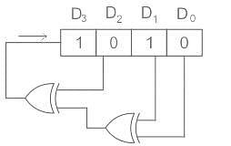
The shift register shown in the figure is initially loaded with the bit pattern 1010. Subsequently, the shift register is clocked, and with each clock pulse the pattern gets shifted by a one-bit position to the right With each shift, the bit at the serial input is pushed to the leftmost position (MSB) After how many clock pulses will the content of the shift register become 1010 again?

Detailed Solution for Test: Shift Registers - 2 - Question 6

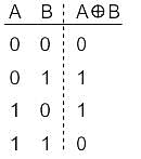
Truth table of X-OR gate:

Analysis:

X = D1 ⊕ D0

D3+ = X ⊕ D2

D2+ = D3

D1+ = D2

D0+ = D1

Test: Shift Registers - 2 - Question 7

What is the output after two clock pulses for a bit sequence 1101 serially entered into a 4-bit parallel out shift register which is initially clear?

Detailed Solution for Test: Shift Registers - 2 - Question 7

Concept:

The data movement from left to right is shown in the below figure:

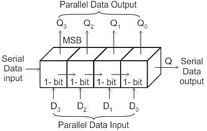
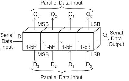
The structure of the SIPO register is:

Basic data movement in a shift register is shown below:

Calculation

Given that the initial content is 0000 and the data is 1101.

After the first clock pulse, the value of the register is 1000.

After the second clock pulse, the value of the register is 0100.

After the third clock pulse, the value of the register is 1010.

After the fourth clock pulse, the value of the register is 1101.

Test: Shift Registers - 2 - Question 8

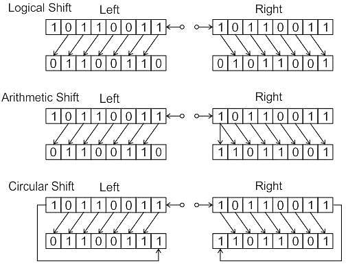
Which of the following is/are the types of shifts in shift registers?

Detailed Solution for Test: Shift Registers - 2 - Question 8

All are the type of Shift Operation therefore option 1 is correct, that is, All of the Options

Logical Shift Left

One position moves each bit to the left one by one

Logical Shift Right

One position moves each bit to the right one by one

Left Arithmetic Shift

One position moves each bit to the left one by one. The empty least significant bit (LSB) is filled with zero and the most significant bit (MSB) is rejected.

Right Arithmetic Shift
One position moves each bit to the right one by one and the least significant bit is rejected and the empty MSB is filled with the value of the previous MSB.

Circular shift

The circular shift circulates the bits in the sequence of the register around both ends without any loss of information.

Test: Shift Registers - 2 - Question 9

Which of the following statements is not correct about a universal shift register?

Detailed Solution for Test: Shift Registers - 2 - Question 9

Shift Register: 

1). A shift register has the capability to store one bit and if another bit is to store, in such a situation it deletes the previous data and stores them.

2). A universal shift register is a bidirectional register whose inputs can be either in serial form or in parallel form. (Option 1 is true)

3). An n-bit shift register consists of ‘N’ number of D flipflops and ‘N’ number of MUX.(Option 3 is correct)

4). The universal shift register has a clear control that clears the contents of the register to 0 and a preset control to set the contents of the register to 1. (Option 4 is correct)

5). The universal shift register does not have an internal clock to synchronize the operations (Option 2 is false)

The basic block diagram of a shift register is as shown:

*Answer can only contain numeric values
Test: Shift Registers - 2 - Question 10

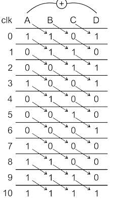
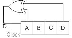
A 4-bit shift register circuit configured for right-shift operation, i.e. Din → A, A → B, B → C, C → D, is shown. If the present state of the shift register is ABCD = 1101, the number of clock cycles required to reach the state ABCD = 1111 is ________.

Detailed Solution for Test: Shift Registers - 2 - Question 10

Input to A is Exor of Previous value of A and D

New Input to B , C, D are previous values of A, B, C respectively.

Total clock cycles required is 10

115 videos|71 docs|58 tests
Information about Test: Shift Registers - 2 Page
In this test you can find the Exam questions for Test: Shift Registers - 2 solved & explained in the simplest way possible. Besides giving Questions and answers for Test: Shift Registers - 2, EduRev gives you an ample number of Online tests for practice

Top Courses for Electrical Engineering (EE)

115 videos|71 docs|58 tests
Download as PDF

Top Courses for Electrical Engineering (EE)