31 Year NEET Previous Year Questions: Semiconductor Electronics - 2 - NEET MCQ
25 Questions MCQ Test Topic-wise MCQ Tests for NEET - 31 Year NEET Previous Year Questions: Semiconductor Electronics - 2

Reverse bias applied to a junction diode [2003]
In semiconductors, at room temperature [2004]
| 1 Crore+ students have signed up on EduRev. Have you? Download the App |
The peak voltage in the output of a half-wavediode rectifier fed with a sinusoidal signalwithout filter is 10V. The d.c. component of theoutput voltage is [2004]

The output of OR gate is 1 [2004]
In a p-n junction photocell, the value of thephoto-electromotive force produced bymonochromatic light is proportional to [2004]
Of the diodes shown in following diagrams, which one is reverse biased ? [2004]
Choose the only false statement from thefollowing [2005]
Carbon, silicon and germanium atoms have fourvalence electrons each. Their valence andconduction bands are separated by energy bandgaps represented by (Eg)C, (Eg)Si and (Eg)Gerespectively. Which one of the followingrelationships is true in their case? [2005]
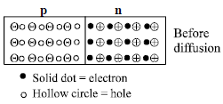
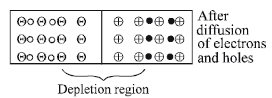
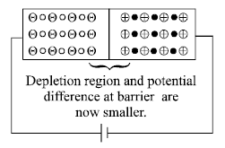
Application of a forward bias to a p–n junction [2005]
Zener diode is used for [2005]
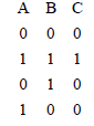
The following figure shows a logic gate circuit with two inputs A and B and the output C. The voltage waveforms of A, B and C are as shown below
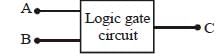
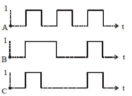
The logic circuit gate is [2006]
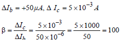
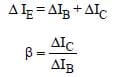
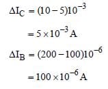
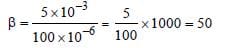
A transistor is operated in common emitterconfiguration at constant collector voltage Vc =1.5V such that a change in the base current from100 μA to 150 μA produces a change in thecollector current from 5 mA to 10 mA. The currentgain (β) is [2006]
A forward biased diode is [2006]
The radius of germanium (Ge) nuclide ismeasured to be twice the radius of 94Be . Thenumber of nucleons in Ge are [2006]
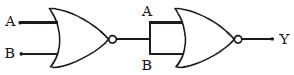
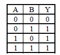
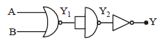
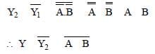
In the following circuit, the output Y for all possible inputs A and B is expressed by the truth table [2007]
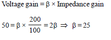
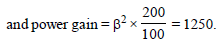
A common emitter amplifier has a voltage gainof 50, an input impedance of 100Ω and an outputimpedance of 200Ω. The power gain of theamplifier is [2007]
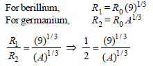
For a cubic crystal structure which one of thefollowing relations indicating the cellcharacteristics is correct? [2007]
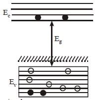
In the energy band diagram of a material shown below, the open circles and filled circles denote holes and electrons respectively. The material is [2007]
The voltage gain of an amplifier with 9% negativefeedback is 10. The voltage gain withoutfeedback will be [2008]
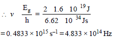
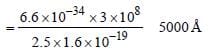
A p-n photodiode is made of a material with aband gap of 2.0 eV. The minimum frequency ofthe radiation that can be absorbed by the materialis nearly [2008]
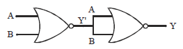
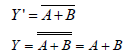
The circuit
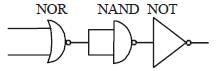
is equivalent to

The symbolic representation of four logic gates are given below : [2009]
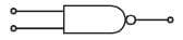
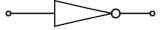
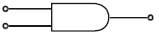
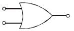
The logic symbols for OR, NOT and NAND gates are respectively:
A p-n photodiode is fabricated from a semiconductor with a band gap of 2.5 eV. It candetect a signal of wavelength [2009]

A transistor is operated in common-emitterconfiguration at Vc = 2 V such that a change inthe base current from 100 μA to 200 μA producesa change in the collector current from 5 mA to10 mA. The current gain is [2009]
The number of beta particles emitted by aradioactive substance is twice the number ofalpha particles emitted by it. The resultingdaughter is an [2009]
 its mass number reduces
|
9 docs|1272 tests
|
Important Questions for 31 Year NEET Previous Year Questions: Semiconductor Electronics - 2
31 Year NEET Previous Year Questions: Semiconductor Electronics - 2 MCQs with Answers
Online Tests for 31 Year NEET Previous Year Questions: Semiconductor Electronics - 2 Topic-wise MCQ Tests for NEET
|
© EduRev
|
Education Revolution
|


Follow Us
|


within 7 days!