Electronics And Communication (Set 2) - ECE 2017 GATE Paper (Practice Test) - Electronics and Communication Engineering (ECE) MCQ
30 Questions MCQ Test GATE ECE (Electronics) Mock Test Series 2025 - Electronics And Communication (Set 2) - ECE 2017 GATE Paper (Practice Test)
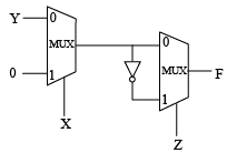
Consider the circuit shown in the figure.

The Boolean expression F implemented by the circuit is
An LTI system with unit sample response  is a
is a
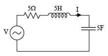
In the circuit shown, V is a sinusoidal voltage source. The current I is in phase with voltage V.


In a DRAM,
Consider an n-channel MOSFET having width W, length L, electron mobility in the channel μn and oxide capacitance per unit area Cox. If gate-to-source voltage VGS = 0.7V, drain-tosource voltage VDS = 0.1V, (μn Cox) = 100μA / V2 , threshold voltage VTH = 0.3 V and (W/L) = 50, then the transconductance gm (in mA/V) is ___________.
Two conducting spheres S1 and S2 of radii a and b (b>a) respectively, are placed far apart and connected by a long, thin conducting wire, as shown in the figure.
For some charge placed on this structure, the potential and surface electric field on S1 are Va and Ea, and that on S2 are Vb and Eb, respectively, which of the following is CORRECT?
For the circuit shown in the figure, P and Q are the inputs and Y is the output.
The logic implemented by the circuit is
An n-channel enhancement mode MOSFET is biased at VGS > VTH and VDS > (VGS - VTH) , where VGS is the gate-to-source voltage, VDS is the drain-to-source voltage and VTH is the threshold voltage. Considering channel length modulation effect to be significant, the MOSFET behaves as a
A connection is made consisting of resistance A in series with a parallel combination of resistances B and C. Three resistors of value 10Ω, 5Ω, 2Ω are provided. Consider all possible permutations of the given resistors into the positions A, B, C, and identify the configurations with maximum possible overall resistance, and also the ones with minimum possible overall resistance. The ratio of maximum to minimum values of the resistances (up to second decimal place) is ____________.
An npn bipolar junction transistor (BJT) is operating in the active region. If the reverse bias across the base – collector junction is increased, then
Consider the state space realization
, with the initial condition
where u(t) denotes the unit step function. The value of
The rank of the matrix
A two – wire transmission line terminates in a television set. The VSWR measured on the line is 5.8. The percentage of power that is reflected from the television set is ______________
The input x(t) and the output y(t) of a continuous-time system are related as
Which of the following statements is incorrect?
The residues of a function
A sinusoidal message signal is converted to a PCM signal using a uniform quantizer. The required signal-to-quantization noise ratio (SQNR) at the output of the quantizer is 40dB. The minimum number of bits per sample needed to achieve the desired SQNR is _______
The general solution of the differential equation in terms of arbitrary
constants K1 and K2 is
Which one of the following graphs shows the Shannon capacity (channel capacity) in bits of a memory less binary symmetric channel with crossover probability P?
The output V0 of the diode circuit shown in the figure is connected to an averaging DC voltmeter. The reading on the DC voltmeter in Volts, neglecting the voltage drop across the diode, is ____________.
Consider the random process X (t) = U+ Vt, where U is a zero-mean Gaussian random variable and V is a random variable uniformly distributed between 0 and 2. Assume that U and V are statistically independent. The mean value of the random process at t = 2 is ____________
For the system shown in the figure, Y(s) / X(s) = __________.
The smaller angle (in degrees) between the planes x + y + z =1 and 2x – y + 2z = 0 is
Consider the circuit shown in the figure. Assume base-to- emitter voltage VBE = 0.8 V and common base current gain (α) of the transistor is unity.
The value of the collector- to – emitter voltage VCE (in volt) is _______.
In the figure, D1 is a real silicon pn junction diode with a drop of 0.7V under forward bias condition and D2 is a zener diode with breakdown voltage of -6.8 V. The input Vin(t) is a periodic square wave of period T, whose one period is shown in the figure.
Assuming 10t << T. where t is the time constant of the circuit, the maximum and minimum values of the output waveform are respectively,
If the vector function is irrotational, then the values of the constants k1, k2 and k3 respectively, are
The un-modulated carrier power in an AM transmitter is 5kW. This carrier is modulated by a sinusoidal modulating signal. The maximum percentage of modulation is 50%. If it is reduced to 40%, then the maximum un-modulated carrier power (in kW) that can be used without overloading the transmitter is ___________
Consider an LTI system with magnitude response
And phase response Arg {H (f)} = -2f.
If the input to the system is
Then the average power of the output signal y (t) is _________.
A MOS capacitor is fabricated on p-type Si (silicon) where the metal work function is 4.1 eV and electron affinity of Si is 4.0 eV. EC-FF = 0.9 eV, where EC and EF are the conduction band minimum and the Fermi energy levels of Si, respectively. Oxide F / cm. oxide thickness tox = 0.1 μm and electronic charge q = 1.6 ×10⁻¹⁹ C. If the measured flat band voltage of the capacitor is -1V, then the magnitude of the fixed charge at the oxidesemiconductor interface, in nC/cm2, is __________.
An electron (q1) is moving in free space with velocity 105 m/s towards a stationary electron (q2) far away. The closest distance that this moving electron gets to the stationary electron before the repulsive force diverts its path is ___________ ×10-8m.
[Given, mass of electron m = 9.11×10⁻³¹kg, charge of electron e = -1.6×10⁻¹⁹C , and permittivity
|
25 docs|263 tests
|


