1 Crore+ students have signed up on EduRev. Have you? Download the App |
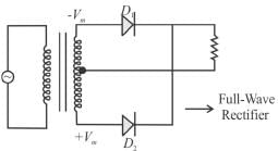
The voltage across a diode in a full-wave rectifier having input voltage of peak value Vm during its non-conducting period is :
During non-conducting period, the voltage across D1 is Vm. = -2Vm.
The correct answer is:
When reverse voltage across silicon diode is changed from 4V to 8 V, what happens to depletion layer?
Under reverse bias (applying a negative voltage to the P-side with respect to the N-side), the potential drop (i.e., voltage) across the depletion region increases. Essentially, majority carriers are pushed away from the junction, leaving behind more charged ions.
When two identical zener diodes are connected in series, what happens to the breakdown voltage of the combination ?
The two zener diodes when connected in series will double the breakdown voltage.
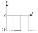
For the clamping network shown below, the resulting output for the applied input will be.
For the first position half of the input signal, the current pass through the diode, hence no current flows through the resistor R, hence, no output voltage is observed and capacitor is charged upto voltage V. For second half (negative), diode blocks the flow of current, hence current pass through resistor R but in opposite direction, hence the potential difference observed across R comes input from signal-V and from the capacitor again in opposite direction, thus making it-2V.
The correct answer is:
The avalanche effect is observed when reverse biased voltage is more than the breakdown voltage.
The correct answer is: the reverse voltage exceeds the breakdown voltage
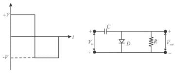
A sinusoidal input voltage Vin of frequency ω is fed to the circuit shown in the figure where if Vm the Peak value of the input voltage, then output voltage (Vout) is.
The circuit looks like a voltage doubler. At the peak of positive half cycle D1 is forward biased and D2 is reverse biased. Ideally, this charges C1 to the peak voltage Vm , with polarity as shown below. At the peak of the negative half cycle, D1 is reverse biased and D2 is forward biased. Because the source and C1 are in series, C2 will try to change towards 2Vm
The correct answer is:
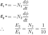
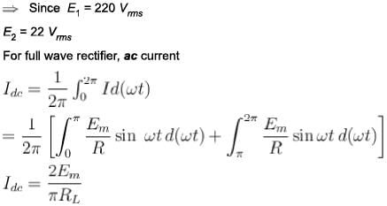
An ac voltage of 220 Vrms is applied to the primary of a 10:1 step-down transformer. The secondary of the transformer is centre tapped and connected to a full-wave rectifier with a load resistance. This dc voltage appearing in the load is.
For step-down transformer,
E2 < E1
(44/π)
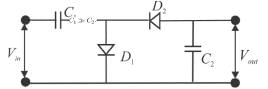
The value of I and V for the circuit shown below are
I = V / R or 5 / 2.5 or 2A
For an ideal diode when it is conducting the potential drop across its terminal is zero
A p-n diode is reverse biased. The resistance measured by an ohm-meter connected across it will be.
In case of reverse biased, the resistance of an ideal p-n diode should be infinity. But practically infinite is not possible and so resistance becomes very high.
The correct answer is: high
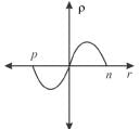
Which graph represents the nature of the curve between charge density p and distance r near the depletion region of p-n junction diode?
Holes will diffuse to right and electrons to left junction initially. Positive holes neutralize the acceptor ions near the function in the p-type silicon and disappeared across junction. Similarly, electrons will be neutralized across n-type by combination with holes of p-type due to diffusion. Thus, across p-type and n-type, there will be lack of majority charge carriers and excess of minority charge carriers. Then, majority charge carriers decreases as we move away from junction.
The Correct answer is