Electrical Engineering (EE) Exam > Electrical Engineering (EE) Tests > Test: DC Load Lines - Electrical Engineering (EE) MCQ
Test: DC Load Lines - Electrical Engineering (EE) MCQ
Test Description
10 Questions MCQ Test - Test: DC Load Lines
Test: DC Load Lines for Electrical Engineering (EE) 2024 is part of Electrical Engineering (EE) preparation. The Test: DC Load Lines questions and answers have been prepared
according to the Electrical Engineering (EE) exam syllabus.The Test: DC Load Lines MCQs are made for Electrical Engineering (EE) 2024 Exam.
Find important definitions, questions, notes, meanings, examples, exercises, MCQs and online tests for Test: DC Load Lines below.
Solutions of Test: DC Load Lines questions in English are available as part of our course for Electrical Engineering (EE) & Test: DC Load Lines solutions in
Hindi for Electrical Engineering (EE) course.
Download more important topics, notes, lectures and mock test series for Electrical Engineering (EE) Exam by signing up for free. Attempt Test: DC Load Lines | 10 questions in 10 minutes | Mock test for Electrical Engineering (EE) preparation | Free important questions MCQ to study for Electrical Engineering (EE) Exam | Download free PDF with solutions
Detailed Solution for Test: DC Load Lines - Question 1
Detailed Solution for Test: DC Load Lines - Question 2
| 1 Crore+ students have signed up on EduRev. Have you? Download the App |
Test: DC Load Lines - Question 3
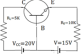
Which of the following depicts the load line for the circuit shown below?

Detailed Solution for Test: DC Load Lines - Question 3
Detailed Solution for Test: DC Load Lines - Question 4
Test: DC Load Lines - Question 5
Which of the following depicts the load line for the given circuit?
Detailed Solution for Test: DC Load Lines - Question 5
Detailed Solution for Test: DC Load Lines - Question 6
Test: DC Load Lines - Question 7
The DC equivalent circuit for an NPN common emitter circuit is.
Detailed Solution for Test: DC Load Lines - Question 7
Test: DC Load Lines - Question 8
What is the other representation of the given PNP transistor connected in common emitter configuration?
Detailed Solution for Test: DC Load Lines - Question 8
Test: DC Load Lines - Question 9
What is the DC characteristic used to prove that the transistor is indeed biased in saturation mode?
Detailed Solution for Test: DC Load Lines - Question 9
Detailed Solution for Test: DC Load Lines - Question 10
Information about Test: DC Load Lines Page
In this test you can find the Exam questions for Test: DC Load Lines solved & explained in the simplest way possible.
Besides giving Questions and answers for Test: DC Load Lines, EduRev gives you an ample number of Online tests for practice
Download as PDF


