Electronics and Communication Engineering (ECE) Exam  >  Electronics and Communication Engineering (ECE) Tests  >  GATE ECE (Electronics) Mock Test Series 2025  >  Test: Electronic Devices - 3 - Electronics and Communication Engineering (ECE) MCQ

Test: Electronic Devices - 3 - Electronics and Communication Engineering (ECE) MCQ


Test Description

10 Questions MCQ Test GATE ECE (Electronics) Mock Test Series 2025 - Test: Electronic Devices - 3

Test: Electronic Devices - 3 for Electronics and Communication Engineering (ECE) 2024 is part of GATE ECE (Electronics) Mock Test Series 2025 preparation. The Test: Electronic Devices - 3 questions and answers have been prepared according to the Electronics and Communication Engineering (ECE) exam syllabus.The Test: Electronic Devices - 3 MCQs are made for Electronics and Communication Engineering (ECE) 2024 Exam. Find important definitions, questions, notes, meanings, examples, exercises, MCQs and online tests for Test: Electronic Devices - 3 below.
Solutions of Test: Electronic Devices - 3 questions in English are available as part of our GATE ECE (Electronics) Mock Test Series 2025 for Electronics and Communication Engineering (ECE) & Test: Electronic Devices - 3 solutions in Hindi for GATE ECE (Electronics) Mock Test Series 2025 course. Download more important topics, notes, lectures and mock test series for Electronics and Communication Engineering (ECE) Exam by signing up for free. Attempt Test: Electronic Devices - 3 | 10 questions in 30 minutes | Mock test for Electronics and Communication Engineering (ECE) preparation | Free important questions MCQ to study GATE ECE (Electronics) Mock Test Series 2025 for Electronics and Communication Engineering (ECE) Exam | Download free PDF with solutions
Test: Electronic Devices - 3 - Question 1

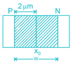
The open-circuit p-n junction diode without any Biasing is shown if NA = 2 × 10¹⁷/cm3, ND = 5 × 10¹⁶/cm3 then the depletion region width (W) is ______μm
Detailed Solution for Test: Electronic Devices - 3 - Question 1

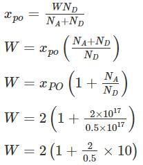
For the p-n junction diode, the depletion region width is given by

W = 10 μm

*Answer can only contain numeric values
Test: Electronic Devices - 3 - Question 2

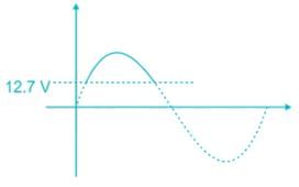
For the diode circuit shown below, If Vs = 24 sin 100πt, and the diode is practical with a cut in voltage of 0.7 V. The conduction angle of the circuit is _______ Degrees. 


Detailed Solution for Test: Electronic Devices - 3 - Question 2

For practical diode

When

Vi > 12 + 0.7 = 12.7 diode conducts

i.e

24 sin θ >12.7

θ > 31.93

Conduction angle = 180 – 2 (31.93)

= 116.12°

1 Crore+ students have signed up on EduRev. Have you? Download the App
Test: Electronic Devices - 3 - Question 3


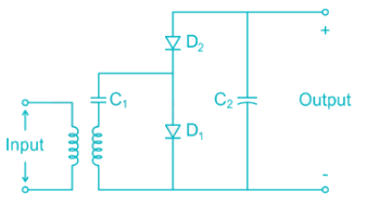
The correct output waveform for the circuit shown if the input is a sinusoidal signal of maximum Amplitude Vmax is 
 

Detailed Solution for Test: Electronic Devices - 3 - Question 3

The circuit shown in a half-wave voltage double During Positive half cycle C1 and D1 Conducts and C is charged to Vmax During Negative half cycle C2 and D2conducts and

 Vout = Vmax + VCl

= 2 Vmax

*Answer can only contain numeric values
Test: Electronic Devices - 3 - Question 4

In the circuit shown, the forward biased LED has a voltage drop of 1.5 volts. If the battery voltage is 6V. Then the power displaced in the resistor R in milliwatts is _________mW. Current through LED is 15mA.


Detailed Solution for Test: Electronic Devices - 3 - Question 4

If r is the internal resistance of LED

Total current = 

As the drop across LED = 1.5 V

Internal resistance r = 
The external resistance to be connected

R = 400 – 100 = 300Ω

Power dissipated in the resistor

I2R = 67.5 mW

Test: Electronic Devices - 3 - Question 5

The voltage regulator circuit using a Zener diode is shown. The Zener diode current is limited in the range 5 ≤ iz ≤ 100 mA 
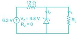

The range of load resistance is

Detailed Solution for Test: Electronic Devices - 3 - Question 5


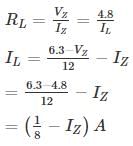
IZ = (125 - IZ)mA

Case A:

IZ = 5 mA

IZ = 120 mA

= 0.12 A


Case B:

IZ = 100 mA

IZ = (125 – 100) mA

= 25 mA

= 0.025 A

*Answer can only contain numeric values
Test: Electronic Devices - 3 - Question 6

For a P±n Si junction the reverse current at room temperature is 0.9 nA/cm2. If donor density is 1015 cm-3 and intrinsic carrier concentration is 1.05 × 10¹⁰. The minority carrier life time is ________ n sec.

[Assume μP = 450 cm2/V-sec, kT = 25mV ] 


Detailed Solution for Test: Electronic Devices - 3 - Question 6

For P±n junction the current density is given by

Substituting

DP = 0.025 × 450

= 11.25

τp = 4.32 × 10⁻⁹ sec

Test: Electronic Devices - 3 - Question 7

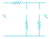
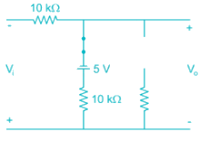
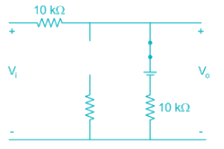
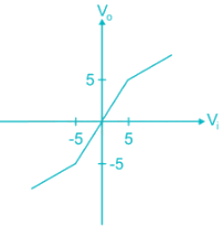
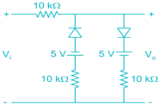
The sketch of output voltage Vo vs. input voltage VI is of from
Detailed Solution for Test: Electronic Devices - 3 - Question 7

For voltages -5V < VI < 5 V both the diodes are off since the diodes are reverse biased.


The output voltage Vo = VI

For VI ≤ -5V

The diode D1 is forward biased, while D2 is reverse biased


For VI ≥ 5 V

The diode D1 is reverse biased, while D2 is forward biased


Drawing sketch of Vo Vs VI

*Answer can only contain numeric values
Test: Electronic Devices - 3 - Question 8

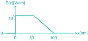
Consider a pn junction at zero bias with an electric distribution as sketched below. Calculate the built-in-potential

Detailed Solution for Test: Electronic Devices - 3 - Question 8

The built in potential is the integral of election field at zero bais:

⇒ 75 × 10-2 V

⇒ 0.75 V

Test: Electronic Devices - 3 - Question 9

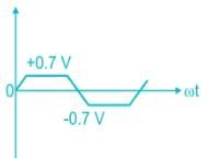
The correct waveform of the output of the given circuit is

Assume the Zener diodes are ideal with threshold voltage Vk = 0.7

Detailed Solution for Test: Electronic Devices - 3 - Question 9

For positive cycle when VI = 0.7 V, the 6 V Zener diode is forward biased while 4 V is reverse biased

For negative cycle VI <-0.7 V, the 6 V Zener diode is reverse biased 4 V Zener diode is forward biased


For -0.7 < VI < 0.7 both the diodes are reverse biased hence Vout = VI

The output waveform will be of form

Test: Electronic Devices - 3 - Question 10

The correct statement regarding depletion and diffusion capacitance is

i) Depletion capacitance is dominant in reverse-bias voltage

ii) Diffusion capacitance is dominant in reverse-bias voltage

iii) The diffusion capacitance is due to a stored charge of minority electrons and minority holes near the depletion region

iv) Depletion capacitance is directly proportional to the width of the depletion region

Detailed Solution for Test: Electronic Devices - 3 - Question 10

Diffusion capacitance is due to transfer of minority carries during forward bias. The minority carries diffuse from one end of junction to other, causing variation of charge with applied voltage. This leads to capacitance, it is present only in forward bias and is significantly higher than depletion capacitance in forward bias.

Depletion capacitance is due to storage of charges in reverse bias junction, which acts like parallel plate capacitance with forward voltage, the depletion width decreases increasing depletion capacitance. It is less than diffusion capacitance in forward bias mode.

25 docs|263 tests
Information about Test: Electronic Devices - 3 Page
In this test you can find the Exam questions for Test: Electronic Devices - 3 solved & explained in the simplest way possible. Besides giving Questions and answers for Test: Electronic Devices - 3, EduRev gives you an ample number of Online tests for practice

Top Courses for Electronics and Communication Engineering (ECE)

Download as PDF

Top Courses for Electronics and Communication Engineering (ECE)