Electronics and Communication Engineering (ECE) Exam  >  Electronics and Communication Engineering (ECE) Tests  >  GATE ECE (Electronics) Mock Test Series 2025  >  Test: Electronic Devices - 6 - Electronics and Communication Engineering (ECE) MCQ

Test: Electronic Devices - 6 - Electronics and Communication Engineering (ECE) MCQ


Test Description

10 Questions MCQ Test GATE ECE (Electronics) Mock Test Series 2025 - Test: Electronic Devices - 6

Test: Electronic Devices - 6 for Electronics and Communication Engineering (ECE) 2024 is part of GATE ECE (Electronics) Mock Test Series 2025 preparation. The Test: Electronic Devices - 6 questions and answers have been prepared according to the Electronics and Communication Engineering (ECE) exam syllabus.The Test: Electronic Devices - 6 MCQs are made for Electronics and Communication Engineering (ECE) 2024 Exam. Find important definitions, questions, notes, meanings, examples, exercises, MCQs and online tests for Test: Electronic Devices - 6 below.
Solutions of Test: Electronic Devices - 6 questions in English are available as part of our GATE ECE (Electronics) Mock Test Series 2025 for Electronics and Communication Engineering (ECE) & Test: Electronic Devices - 6 solutions in Hindi for GATE ECE (Electronics) Mock Test Series 2025 course. Download more important topics, notes, lectures and mock test series for Electronics and Communication Engineering (ECE) Exam by signing up for free. Attempt Test: Electronic Devices - 6 | 10 questions in 30 minutes | Mock test for Electronics and Communication Engineering (ECE) preparation | Free important questions MCQ to study GATE ECE (Electronics) Mock Test Series 2025 for Electronics and Communication Engineering (ECE) Exam | Download free PDF with solutions
Test: Electronic Devices - 6 - Question 1

The finer resolution in lithography can be obtained using

Detailed Solution for Test: Electronic Devices - 6 - Question 1

Smaller is the wave length used in lithography, better is the resolution.

Among the given options, x-rays have minimum wavelength and are expected to give best resolution.

Note: X-rays are presently not used because of increased cost associated while using them.

*Answer can only contain numeric values
Test: Electronic Devices - 6 - Question 2

An ideal solar cell has a short-circuit current of 50 mA and an open circuit voltage of 0.7 V under full illumination. The power delivered to a load of 1 kΩ is ________ mW


Detailed Solution for Test: Electronic Devices - 6 - Question 2

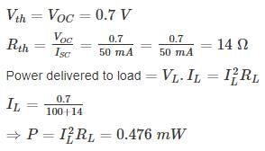
Given,

VOC = 0.7 V, ISC = 50 mA

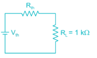
Drawing equivalent circuit


1 Crore+ students have signed up on EduRev. Have you? Download the App
Test: Electronic Devices - 6 - Question 3

The wavelength of the emitted radiation by an electron while transferring from one energy state of -15eV to other states of -5eV is approximately(in nanometer)

Detailed Solution for Test: Electronic Devices - 6 - Question 3

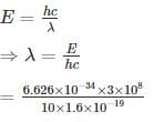
The electron travelling from -15eV state to -5eV state radiate 10 eV energy as photon whose wavelength λ is given by

= 124.2 nm

*Answer can only contain numeric values
Test: Electronic Devices - 6 - Question 4

A solar cell has a short circuit current of 10 mA and open circuit voltage of 0.9 V. The maximum power delivered by the solar cell is _________ mV. Given fill factor as 0.8.


Detailed Solution for Test: Electronic Devices - 6 - Question 4

The maximum power delivered Pm = Vm. Im = f.f × VOC­ ISC

= 0.8 × 0.9 × 10 mA

= 7.2 mW

Test: Electronic Devices - 6 - Question 5

The smallest feature that can be printed with adequate control using photolithography in controlled by

(a) The smallest image that can be projected on the wafer

(b) Resolving capability of photoresist

(c) Temperature of wafer

(d) The energy of Ion Implantation beam.

The correct statement is

Detailed Solution for Test: Electronic Devices - 6 - Question 5

The smallest feature is limited by two Basic limits

a. Smallest Image that can be projected on water.

b. Resolving capability of photo resist

*Answer can only contain numeric values
Test: Electronic Devices - 6 - Question 6

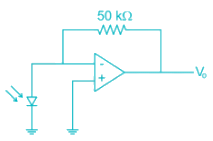
A photo – detector circuit is given in the figure. The photo diode has an active area of 10-2 cm2 and sensitivity of 0.65 A/w. When light of intensity 20 mW/cm2 falls on the photo diode, the output Vo is _______

Detailed Solution for Test: Electronic Devices - 6 - Question 6

The current generated I = R.W

R = sensitivity

W = light power incident

I = 0.65 × 10-2 × 20 mW/cm2

= 0.65 × 10-2 × 10

= 0.13 mA

Output voltage form inverting Op-Amp

Vo = -0.13 × 10-3 × 50 × 103

= -6.5 V

Test: Electronic Devices - 6 - Question 7

Consider the following statements about thermal diffusion of dopants in IC fabrication.

a) Thermal diffusion should be carried out at later stages of the IC fabrication process

b) The lithographic mask used for diffusion should be of hard masks like oxide or nitride

Detailed Solution for Test: Electronic Devices - 6 - Question 7
  • To speed the diffusion, process the wafer has to be heated at 1000°C. Thus, the mask used should have high meting point and hence hard masks of oxide & nitrides are used.
  • Thermal diffusion cannot be used at later stages of the fabrication process because there could be a number of layers that might not be able to withstand high temperature.
*Answer can only contain numeric values
Test: Electronic Devices - 6 - Question 8

A photo diode is illuminated by light with 700 nm wavelength and power of 4 mW. If the open circuit current produced is 1mA then the internal quantum efficiency of photo diode is


Detailed Solution for Test: Electronic Devices - 6 - Question 8

Current generated I = P0 × R

Given P0 = 4 mw

Responsivity  

⇒ η ≃ 0.443

Test: Electronic Devices - 6 - Question 9

Match th4e various process in CMOS fabrication with appropriate description in second list
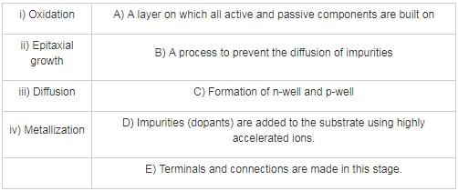
Detailed Solution for Test: Electronic Devices - 6 - Question 9

Oxidation:
- Oxidation of SI water to form SiO2
- Acts as barrier for diffusion of impurities and contamination
- Can be used to fix shape of transistor

Epitaxial growth:
- A layer is built on substrate (n-type layer on p-type substrate and vice versa)
- All active ξ passive components, like transistor, bias resistors and diodes are fabricated on this layer.

Diffusion:
- Dopant impurities are diffused onto epitaxial layer to form terminals of transistor like, drain, source, gate etc.
- N-well, P-well are created using this process.
- Done at high temperature
- Depth of diffusion dependant on time of diffusion
- Ion implantation is also used for adding dopants, but the method is by bombarding Si wafer with accelerated ions.

Metallization:
- A thin metal (mostly aluminium) layer is added to form interconnection of components and Ohmic contacts

*Answer can only contain numeric values
Test: Electronic Devices - 6 - Question 10

A Ga – As LED has a refractive index of 3.6 and is surrounded by air (μ = 1). If the bandgap of Ga – As is 1.43. Then out of 500 photons generated in Ga – As The number of photons emitted out of the specimen are _____


Detailed Solution for Test: Electronic Devices - 6 - Question 10

The external quantum efficiency is given by the relation

ηs = 3.6

ηa = 1

ηext = 0.0193

Out of every 100 photons generated in Ga – As, only 1.93 are emitted out of the specimen.

for 500 photons → 9.5 emitted

Taking greatest integer value

[9.5] = 9

25 docs|263 tests
Information about Test: Electronic Devices - 6 Page
In this test you can find the Exam questions for Test: Electronic Devices - 6 solved & explained in the simplest way possible. Besides giving Questions and answers for Test: Electronic Devices - 6, EduRev gives you an ample number of Online tests for practice

Top Courses for Electronics and Communication Engineering (ECE)

Download as PDF

Top Courses for Electronics and Communication Engineering (ECE)