Test: MOSFET-1 - Electronics and Communication Engineering (ECE) MCQ


Test Description

10 Questions MCQ Test GATE ECE (Electronics) Mock Test Series 2025 - Test: MOSFET-1

Test: MOSFET-1 for Electronics and Communication Engineering (ECE) 2024 is part of GATE ECE (Electronics) Mock Test Series 2025 preparation. The Test: MOSFET-1 questions and answers have been prepared according to the Electronics and Communication Engineering (ECE) exam syllabus.The Test: MOSFET-1 MCQs are made for Electronics and Communication Engineering (ECE) 2024 Exam. Find important definitions, questions, notes, meanings, examples, exercises, MCQs and online tests for Test: MOSFET-1 below.
Solutions of Test: MOSFET-1 questions in English are available as part of our GATE ECE (Electronics) Mock Test Series 2025 for Electronics and Communication Engineering (ECE) & Test: MOSFET-1 solutions in Hindi for GATE ECE (Electronics) Mock Test Series 2025 course. Download more important topics, notes, lectures and mock test series for Electronics and Communication Engineering (ECE) Exam by signing up for free. Attempt Test: MOSFET-1 | 10 questions in 30 minutes | Mock test for Electronics and Communication Engineering (ECE) preparation | Free important questions MCQ to study GATE ECE (Electronics) Mock Test Series 2025 for Electronics and Communication Engineering (ECE) Exam | Download free PDF with solutions
Test: MOSFET-1 - Question 1

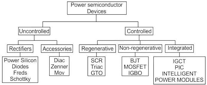
Which of the following does NOT belong to the category of semi-controlled devices?

Detailed Solution for Test: MOSFET-1 - Question 1

Thyristor (Controlled & Semi-controlled device):

  • Thyristors are a broad classification of bipolar-conducting semiconductor devices having four (or more) alternating N-P-N-P layers.
  • It acts exclusively as a bistable switch and starts conducting when the gate receives a current trigger, and continues to conduct until the voltage across the device is reversed biased, or until the voltage is removed by some external circuitry.

Classification of thyristor family:

  • Among the following options, MOSFET does not belong to the Controlled & Semi-controlled device family.
Test: MOSFET-1 - Question 2

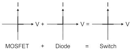
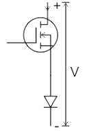
The figure shows a composite switch consisting of a power MOSFET in series with a power diode. Assuming that the MOSFET and the diode are ideal, the I-V characteristic of the composite switch is:
Detailed Solution for Test: MOSFET-1 - Question 2

In a series connection, the IV characteristic is obtained by the intersection of current and union of voltage.

Therefore, option 4 is correct.

1 Crore+ students have signed up on EduRev. Have you? Download the App
Test: MOSFET-1 - Question 3

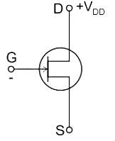
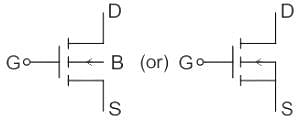
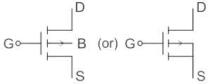
Identify the device based on the given symbol.

Detailed Solution for Test: MOSFET-1 - Question 3

FET is classified based on the channel in each type.
Based on the channel there are two types:
1) n – channel FET
2) p – channel FET
Based on the formation of the channel
1) JFET
2) Depletion  MOSFET
3) Enhancement MOSFET
Field Effect Transistor also has the fourth terminal which is called as “ Body or Substrate”
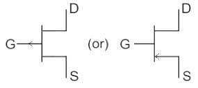
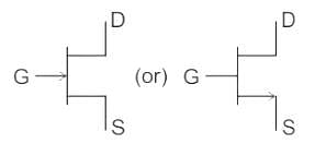
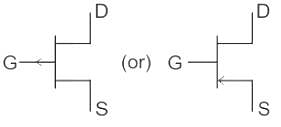
n – channel JFET


p – Channel JFET

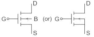
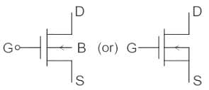
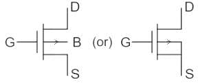
p – channel Depletion MOSFET

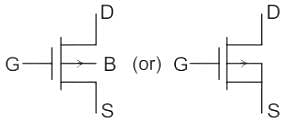
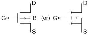
n – Channel Enhancement MOSFET

p – channel Enhancement MOSFET

Test: MOSFET-1 - Question 4

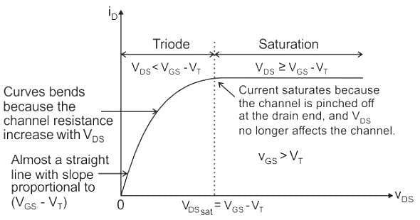
In a power MOSFET, pinch-off occurs when (VDS is the drain to source voltage, VGS is the gate to source voltage VT is the threshold voltage):

Detailed Solution for Test: MOSFET-1 - Question 4


As shown in the above figure in a power MOSFET, pinch-off occurs when VDS = VGS - VT
Where, VDS = Drain to source voltage
VGS = Gate to source voltage
VT = Threshold voltage
In power MOSFET when VDS < VGS - VT, then power MOSFET works in the triode region.
In power MOSFET when VDS > VGS - VT, then power MOSFET works in the saturation region.

Test: MOSFET-1 - Question 5

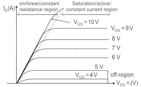
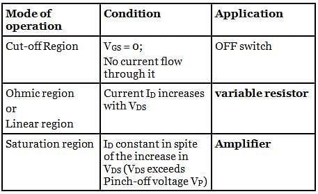
A ‘MOSFET’ acts as amplifier in its-

Detailed Solution for Test: MOSFET-1 - Question 5

MOSFET:
MOSFET stands for Metal Oxide Semiconductor Field Effect Transistor.
It is a majority carrier device and also called as Voltage controlled current device (VGS control the current ID)

Operation of the MOSFET:
The drain characteristics or the plot between ID and VDS is shown below


The drain characteristics are shown in below tabular form.

VGS = Gate-Source voltage
ID = Drain current
VDS = Drain-Source voltage

Test: MOSFET-1 - Question 6

Which of the following is the fastest switching device?

Detailed Solution for Test: MOSFET-1 - Question 6
  • MOSFETs are majority carrier devices that mean flow of current inside the device is carried out either flow of electrons (N-Channel MOSFET) or flow of holes (P-Channel MOSFET).
  • So, when the device turns off, the reverse recombination process will not happen. It leads to short turn ON/OFF times.
  • As switching time is less, loss associated with it less and hence it gives the highest switching speed.
*Answer can only contain numeric values
Test: MOSFET-1 - Question 7

Consider an n-channel metal-oxide-semiconductor field-effect transistor (MOSFET) with a gate-to-source voltage of 1.8 V. Assume that W/L=4, μnCox = 70 x 10-6 AV-2, the threshold voltage is 0.3 V, and the channel length modulation parameter is 0.09 V−1. In the saturation region, the drain conductance (in micro seimens) is ________.


Detailed Solution for Test: MOSFET-1 - Question 7

For a MOSFET in saturation, the current is given by:

W = Width of the Gate
Cox = Oxide Capacitance
μ = Mobility of the carrier
L = Channel Length
Vth = Threshold voltage

Calculation:
The drain conductance (gd) is calculated as the rate of change of drain current with respect to the Drain to source voltage, i.e.

Putting on the respective values, we get:

Test: MOSFET-1 - Question 8

Given, Vgs is the gate-source voltage, Vds is the drain source voltage, and Vth is the threshold voltage of an enhancement type NMOS transistor, the conditions for transistor to be biased in saturation are

Detailed Solution for Test: MOSFET-1 - Question 8

At Vgs = 0, no current flows through the MOS transistors channel because the field effect around the gate is insufficient to create or open the n-type channel. Then the transistor is in its cut-off region acting as an open switch.

As we now gradually increase the positive gate-source voltage Vgs, the field effect begins to enhance the channel regions conductivity and there becomes a point where the channel starts to conduct. This point is known as the threshold voltage Vth. As we increase Vgs more positive, the conductive channel becomes wider (less resistance) with the amount of drain current (Id).

Therefore, the n-channel enhancement MOSFET will be in its cut-off mode when the gate-source voltage (VGS) is less than its threshold voltage level (Vth) and its channel conducts or saturates when Vgs is above this threshold level.

Test: MOSFET-1 - Question 9

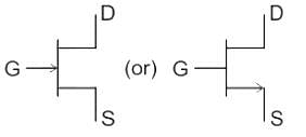
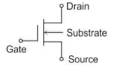
The figure shown below represents

Detailed Solution for Test: MOSFET-1 - Question 9

FET is classified based on the channel in each type.

Based on the channel there are two types:

1) n – channel FET

2) p – channel FET

Based on the formation of the channel

1) JFET

2) Depletion  MOSFET

3) Enhancement MOSFET

Field Effect Transistor also has the fourth terminal which is called as “ Body or Substrate”

n – channel JFET


p – Channel JFET


n – channel Depletion MOSFET


p – channel Depletion MOSFET


n – Channel Enhancement MOSFET


p – channel Enhancement MOSFET

In Depletion MOSFET channel is initially formed whereas in Enhancement MOSFET it is not. So channel in Enhancement MOSFET is represented by the dotted symbol.
Conclusion: From the given figure as the channel is thick line it is Depletion MOSFET. The direction of the arrow is inside, so it represents n – channel.

Test: MOSFET-1 - Question 10

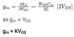
Trans conductance of MOSFET in linear region can be approximated by ______

Detailed Solution for Test: MOSFET-1 - Question 10

For a MOSFET operating in the linear region, the current is given by:


W = Width of the Gate
Cox = Oxide Capacitance
μ = Mobility of the carrier
L = Channel Length
Vth = Threshold voltage
The transconductance is defined as the change in drain current for a given change in Gate-to-source voltage, i.e.

Differentiation equation (1) with VGS we get:

Hence option (2) is the correct answer.

25 docs|263 tests
Information about Test: MOSFET-1 Page
In this test you can find the Exam questions for Test: MOSFET-1 solved & explained in the simplest way possible. Besides giving Questions and answers for Test: MOSFET-1, EduRev gives you an ample number of Online tests for practice

Top Courses for Electronics and Communication Engineering (ECE)

Download as PDF

Top Courses for Electronics and Communication Engineering (ECE)