1 Crore+ students have signed up on EduRev. Have you? |
Diode acts as a short circuit when switched from forward to reverse bias for some time due to______
When a diode is switched suddenly, it persists the conducting property for a short time in its reverse bias also. This leads to excess minority charge carrier settlement at potential barrier. Hence acts as a short circuit.
The time period for which diode remains in conduction state even in reverse direction is called storage time. The time elapsed to return the non conduction state is called transition time. Their sum is called reverse recovery time.
Switching leads to move holes in P region to N region as minority carriers. Removal of this accumulation determines switching speed. P+ regards to a diode in which the p type is doped excessively.
Time taken for a diode to reach 90% of its final value when switched from steady state is______
Time constant = RC. To reach 90% of the final value, time taken is 2.2 of RC. Time constant is the time required to discharge the capacitor, through the resistor, by 36.8%.
Which of the following are true?
1) In reverse bias, the diode undergoes stages of storage and transition times
2) Minority charge carriers accumulation makes the diode as a short circuit
3) Storage time is the sum of recovery and transition times
When a diode is switched from forward to reverse bias, storage and transition times takes place. The accumulation time or the life time of minority carriers makes it a short circuit. The conduction property is holds for a short period of time in reverse bias also.
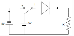
In a circuit below, the switch is at position 1 at t<0 and at position 2 when t=0. Assume diode has zero voltage drop and storage time. For 0<t<ts, the VR at 1k ohm resistor is given by_____
At position ‘1’ when connected to +5V, the diode is forward biased and acts as a short circuit. So, VR is 5V. For 0<t<ts VR is -5V as the diode is in reverse bias. But it holds the conductive property within the storage time period. So, V is -5V.
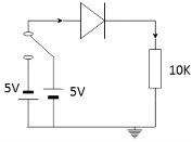
The switch is at position shown in the figure initially and steady state is from t=0 to t=to. The switch suddenly is thrown to the other position. The current flowing through the 10K resistor from t=0 is?
Initially, the diode is in forward bias. When suddenly switched to reverse bias, upto a storage time limit, it conducts during storage time period.
We know that, current I=V/R=-20/10K=-2mA.
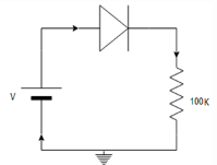
A PN junction diode with 100Ω resistor is forward biased such that 100A current flows. If voltage across this combination is instantaneously reversed to 10V at t=0, the reverse current that flows through diode at t=0 is?
At t=0, V=-10V. During storage time, current still flows.
We know that,
current I=V/R=10/100Ω=100mA from N to P region.
The delay in switching between the ON and OFF states is due to _________
When switched instantaneously it stays in a quasi state i.e.., temporary state which stores charges. The delay is produced due to this charge settlement. The diode needs to discharge these excess carriers in order to return the non conduction stage.
When the current increases the depletion layer decreases and the storage and transition time decreases. A decreased depletion layer can easily discharge the excess carrier and thereby lessens the delay time.
11 videos|57 docs|108 tests
|
Use Code STAYHOME200 and get INR 200 additional OFF
|
Use Coupon Code |
11 videos|57 docs|108 tests
|
|
|
|
|
|
|
|
|
|