Test: Basic FET Amplifiers- 2 - Electrical Engineering (EE) MCQ
10 Questions MCQ Test Topicwise Question Bank for Electrical Engineering - Test: Basic FET Amplifiers- 2
In the common drain amplifier shown below, if RS = 4 KΩ, RG = 10 MΩ, μ = 50 and rd = 35 KΩ then the voltage gain Av of the amplifier is approximately equal to


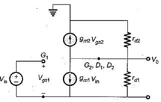
The value of V0/Vin for the circuit shown below is (Assume M1 in saturation)


| 1 Crore+ students have signed up on EduRev. Have you? Download the App |
Consider the following statements:
1. In most linear applications of field-effect transistors the device is operated in the. constant-current portion of its output characteristics.
2. In the region before pinch-off, where VDS is small, the FET is useful as a voltage variable resistors (VVR).
3. The VVR can be used in AGC amplifier to vary the voltage gain of multistage amplifier.
Q. Which of the above statements is/are correct?
1. In most linear applications of field-effect transistors the device is operated in the. constant-current portion of its output characteristics.
2. In the region before pinch-off, where VDS is small, the FET is useful as a voltage variable resistors (VVR).
3. The VVR can be used in AGC amplifier to vary the voltage gain of multistage amplifier.
In the saturation region, the ID - VGS characteristics of a MOSFET are
The source-bias circuit provides DC biasing for the FET. The resistance from gate to ground (RS) in that circuit is necessary because, without it,
In an FET common-source high frequency amplifier, which one of the following is the correct expression for input capacitance Ci ?
A JFET is set up as a source follower. Given, μ = 200, rd = 100 kΩ and source load resistance RL = 1 kΩ. The output resistance R0 is given approximately by
A FET tuned amplifier with gm = 5 mA/V, rd = 20 kΩ has a resonant impedance of 20 kΩ. The gain at resonance is given by
The transconductance for a JFET having IDSS = 8 mA, VP = -4 V and biased to operate at VGS = - 1.8 volt will be given by


 in saturation region,therefore the ID - VGS characteristics of a MOSFET are quadratic as evident from the above equation.


