Electronics and Communication Engineering (ECE) Exam  >  Electronics and Communication Engineering (ECE) Tests  >  GATE ECE (Electronics) Mock Test Series 2025  >  Test: P-Type Semiconductor - Electronics and Communication Engineering (ECE) MCQ

Test: P-Type Semiconductor - Electronics and Communication Engineering (ECE) MCQ


Test Description

5 Questions MCQ Test GATE ECE (Electronics) Mock Test Series 2025 - Test: P-Type Semiconductor

Test: P-Type Semiconductor for Electronics and Communication Engineering (ECE) 2024 is part of GATE ECE (Electronics) Mock Test Series 2025 preparation. The Test: P-Type Semiconductor questions and answers have been prepared according to the Electronics and Communication Engineering (ECE) exam syllabus.The Test: P-Type Semiconductor MCQs are made for Electronics and Communication Engineering (ECE) 2024 Exam. Find important definitions, questions, notes, meanings, examples, exercises, MCQs and online tests for Test: P-Type Semiconductor below.
Solutions of Test: P-Type Semiconductor questions in English are available as part of our GATE ECE (Electronics) Mock Test Series 2025 for Electronics and Communication Engineering (ECE) & Test: P-Type Semiconductor solutions in Hindi for GATE ECE (Electronics) Mock Test Series 2025 course. Download more important topics, notes, lectures and mock test series for Electronics and Communication Engineering (ECE) Exam by signing up for free. Attempt Test: P-Type Semiconductor | 5 questions in 15 minutes | Mock test for Electronics and Communication Engineering (ECE) preparation | Free important questions MCQ to study GATE ECE (Electronics) Mock Test Series 2025 for Electronics and Communication Engineering (ECE) Exam | Download free PDF with solutions
Test: P-Type Semiconductor - Question 1

Which of the following can be used in the fabrication of p-type semiconductor?

Detailed Solution for Test: P-Type Semiconductor - Question 1

Semiconductor: 

  • Semiconductors are materials that have a conductivity between conductors and insulators.
  • Semiconductors are made of compounds such as gallium arsenide or pure elements, such as germanium or silicon.

There are two types of semiconductors:

  • ​N-type Semiconductor
  • P-type Semiconductor

Test: P-Type Semiconductor - Question 2

For P-type semiconductor, the dopant is

Detailed Solution for Test: P-Type Semiconductor - Question 2

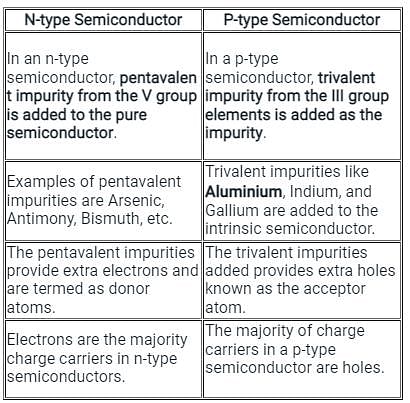
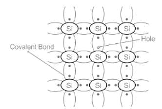
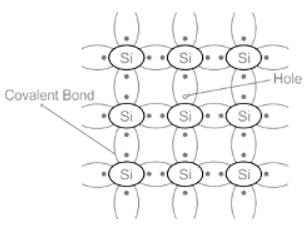
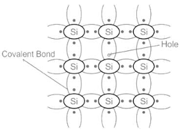
In a P-type semiconductor material, holes are generated because a trivalent impurity atom has one less electron than the surrounding silicon atom. Thus, leaving a vacancy in a covalent bond that acts as a hole. The presence of a hole does not make the semiconductor material positively charge because in an impurity atom, no. of electron and proton is equal before and after the doping, and the same applies for the silicon atom.

Thus, p-type semiconductor crystal remains neutral.

Important Points:

  • Extrinsic P-type Semiconductor is formed when a trivalent impurity is added to a pure semiconductor.
  • Example of trivalent impurity is Boron, Gallium, and Indium.
  • Trivalent impurity like boron has 3 valence electrons.
  • Each atom of the impurity fits in the silicon crystal by forming covalent bonds with the surrounding silicon atoms.
  • The dopant boron atom has one less electron than surrounding silicon and thus vacancy is generated that acts as a hole.

1 Crore+ students have signed up on EduRev. Have you? Download the App
Test: P-Type Semiconductor - Question 3

Majority carriers of P type material

Detailed Solution for Test: P-Type Semiconductor - Question 3

P-type semiconductor:

  • Extrinsic P-type Semiconductor is formed when a trivalent impurity is added to a pure semiconductor
  • Example of trivalent impurity are Boron, Gallium, and Indium
  • Trivalent impurity like boron has 3 valence electrons.
  • Each atom of the impurity fits in the silicon crystal by forming covalent bonds with the surrounding silicon atoms
  • The dopant boron atom has one less electron than surrounding silicon and thus vacancy is generated that acts as a hole
  • Therefore, holes are in majority in the p-type semiconductors. 


Important Point

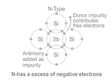
Pentavalent impurities:

Impurity atoms with 5 valence electrons produce n-type semiconductors by contributing an extra electron.

This is as explained in the figure:

*Answer can only contain numeric values
Test: P-Type Semiconductor - Question 4

A sample of GaAs doped with NA = 1017 cm-3. For GaAs intrinsic concentration is n = 2.2 × 106 cm-3, mobility of electron is μn = 5300 cm2/V-sec, and mobility of hole is μp = 230 cm2/V sec.

If the sample is illuminated such that the excess electron concentration is 1016 cm-3. What will the conductivity [in (Ω-cm)-1] of this sample, when the light is ON?  


Detailed Solution for Test: P-Type Semiconductor - Question 4

Concept:

The conductivity for a doped semiconductor is obtained as:

σ = q n0 μn = q p0 μp

where,

ni = Intrinsic carrier concentration.

μn = electron mobility

μp = Hole mobility

When a semiconductor crystal is optically excited, one hole is created for every electron, i.e. electron-hole pass are created.  

Application:

When the light is ON, excess electron and holes are generated in pairs, i.e.

Δp = Δn = 1016 cm3

Before Illumination:

NA = 1017 cm-3 and ni = 2.2 × 106 cm-3

Since NA ≫ ni, the excess hole concentration at thermal equilibrium will be:

p0 = NA = 1017 cm-3

The electron concentration using mass-action law is obtained as:

The electron concentration before illumination is negligible.

After illumination:

When an electron is generated optically, one hole is also created, i.e. they always occur in pairs.

∴ The excess hole concentration and excess electron concentration will be the same, i.e.

Δp = Δn = 1016 cm-3

Now, the electron and hole concentration after illumination will be:

n = n0 + Δn

n = 4.8 × 10⁻⁵ + 1016

n = 1016

Similarly,

p = p0 + Δp

p = 1017 + 1016 cm-3

p = 11 × 1016 cm-3

∴ the conductivity of the given sample when the light is ON will be:

σ = q(n0 + Δnn + q(p0 + Δpp

σ = q[(1016n + (11 × 1016p]

= (1.6 × 10⁻¹⁹) (1016 × 5300 + (11 × 1016) (230))

= 1.6 × 10⁻¹⁹ (5.3 × 10¹⁹ + 2.53 × 10¹⁹)

= 1.6 × (5.3 + 2.53)

σ = 12.528 (Ω-cm)-1

Test: P-Type Semiconductor - Question 5

Doping material for p-type semiconductor is:

Detailed Solution for Test: P-Type Semiconductor - Question 5
  • Extrinsic p-Type Semiconductor is formed when a trivalent impurity is added to a pure semiconductor.
  • Example of trivalent impurity are Boron, Gallium, and Indium
  • Trivalent impurity like boron, have 3 valence electrons.
  • Each atom of the impurity fits in the silicon crystal by forming covalent bonds with the surrounding silicon atoms.
  • The dopant boron atom has one less electron than surrounding silicon and thus vacancy is generated that acts as a hole.

25 docs|263 tests
Information about Test: P-Type Semiconductor Page
In this test you can find the Exam questions for Test: P-Type Semiconductor solved & explained in the simplest way possible. Besides giving Questions and answers for Test: P-Type Semiconductor, EduRev gives you an ample number of Online tests for practice

Top Courses for Electronics and Communication Engineering (ECE)

Download as PDF

Top Courses for Electronics and Communication Engineering (ECE)