Electronics and Communication Engineering (ECE) Exam  >  Electronics and Communication Engineering (ECE) Tests  >  GATE ECE (Electronics) Mock Test Series 2025  >  Test: The PN - Junction - Electronics and Communication Engineering (ECE) MCQ

Test: The PN - Junction - Electronics and Communication Engineering (ECE) MCQ


Test Description

20 Questions MCQ Test GATE ECE (Electronics) Mock Test Series 2025 - Test: The PN - Junction

Test: The PN - Junction for Electronics and Communication Engineering (ECE) 2024 is part of GATE ECE (Electronics) Mock Test Series 2025 preparation. The Test: The PN - Junction questions and answers have been prepared according to the Electronics and Communication Engineering (ECE) exam syllabus.The Test: The PN - Junction MCQs are made for Electronics and Communication Engineering (ECE) 2024 Exam. Find important definitions, questions, notes, meanings, examples, exercises, MCQs and online tests for Test: The PN - Junction below.
Solutions of Test: The PN - Junction questions in English are available as part of our GATE ECE (Electronics) Mock Test Series 2025 for Electronics and Communication Engineering (ECE) & Test: The PN - Junction solutions in Hindi for GATE ECE (Electronics) Mock Test Series 2025 course. Download more important topics, notes, lectures and mock test series for Electronics and Communication Engineering (ECE) Exam by signing up for free. Attempt Test: The PN - Junction | 20 questions in 60 minutes | Mock test for Electronics and Communication Engineering (ECE) preparation | Free important questions MCQ to study GATE ECE (Electronics) Mock Test Series 2025 for Electronics and Communication Engineering (ECE) Exam | Download free PDF with solutions
Test: The PN - Junction - Question 1

In forward biasing of the p-n junction

Detailed Solution for Test: The PN - Junction - Question 1

Concept:
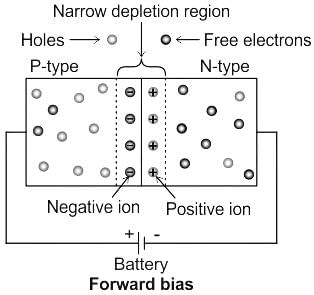
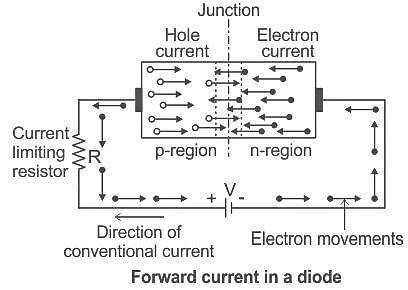
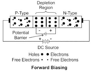
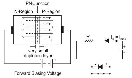
Forward Biased PN Junction Diode: When a diode is connected in a Forward Bias condition, a negative voltage is applied to the N-type material and a positive voltage is applied to the P-type material.
When this external voltage becomes greater than the value of the potential barrier for diode, that is approx 0.3 volts for germanium and 0.7 volts for silicon, the potential barriers opposition will be overcome and the current will start to flow. This is the conventional current.

Explanation:
Forward Bias:


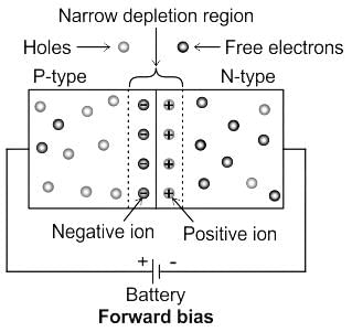
  • When the negative terminal of the battery is connected to the N – side and the positive terminal to P –side, then the connection is called forward bias. Hence option 1 is correct.
  • In forward biasing, the applied voltage V of the battery mostly drops across the depletion region and the voltage drops across the p-side and n-side of the p-n junction is negligibly small.
  • It is because the resistance of the depletion region is very high as it has no free charge carriers.

Note:

  • In forward biasing the forward voltage opposes the potential barrier Vb. As a result of it, the potential barrier height is reduced and the width of the depletion layer decreases.
  • As forward voltage is increased, at a particular value the depletion region becomes very much narrow such that a large number of majority charge carriers can cross the junction.
Test: The PN - Junction - Question 2

A light emitting p-n junction can also be made to emit _________ and thus can serve as a laser.

Detailed Solution for Test: The PN - Junction - Question 2

Concept:
Emission:

  • Light can be produced by the matter in an excited state and, as we will show, excitation can come from various sources.
  • The atoms and molecules that makeup matter typically emit light at characteristic energies.
  • The light emission can be spontaneous or stimulated.

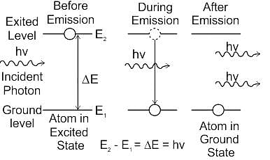
Stimulated emission:

  • The process by which an incoming photon of a specific frequency can interact with an excited atomic electron, causing it to drop to a lower energy level.
  • The liberated energy transfers to the electromagnetic field, creating a new photon with a frequency, polarization, and direction of travel that are all identical to the photons of the incident wave.
     

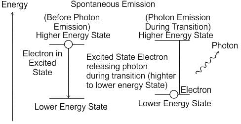
Spontaneous emission:

  • When an isolated atom is excited into a high-energy state, it generally remains in the excited state for a short time before emitting a photon and transitioning to a lower-energy state.

This fundamental process is called spontaneous emission.
Explanation:
Light emitting in a PN junction:

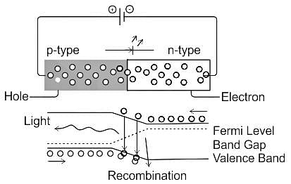
  • Light is released in the form of a photon in the recombination process. 
  • A light-emitting p-n junction can also be made to emit stimulated emission.
  • This emission can serve as a laser.
1 Crore+ students have signed up on EduRev. Have you? Download the App
Test: The PN - Junction - Question 3

The resistance of a p - n junction in forward bias is –

Detailed Solution for Test: The PN - Junction - Question 3

Concept:

  • When a p-type semiconductor crystal is brought into close contact with an n-type semiconductor crystal, the resulting arrangement is called p-n junction diode.

Explanation:


Forward Bias:

  • When the negative terminal of the battery is connected to the N – side and the positive terminal to P –side, then the connection is called forward bias.
  • In forward biasing, the applied voltage V of the battery mostly drops across the depletion region and the voltage drops across the p-side and n-side of the p-n junction is negligibly small.
  • It is because the resistance of the depletion region is very high as it has no free charge carriers.
  • A p - n junction diode allows electric current in one direction and blocks electric current in another direction.
  • It allows electric current when it is forward biased and blocks electric current when it is reverse biased.
  • An actual diode offers a very small resistance (ideally zero but actually very low) when forward biased and is called forward resistance. Therefore option C is correct.
Test: The PN - Junction - Question 4

The reason of current flow in p-n junction in forward bias is:

Detailed Solution for Test: The PN - Junction - Question 4

Concept:
Forward Bias: 

  • When the negative terminal of the battery is connected to the N - side and the positive terminal to P - side the connection is called forward bias.

Explanation:

  • In forward biasing, the applied voltage V of the battery mostly drops across the depletion region and the voltage drops across the p-side and n-side of the p-n junction is negligibly small.
  • It is due to the fact that the resistance of the depletion region is very high as it has no free charge carriers.
  • Due to concentration difference, holes try to diffuse from p-side to the n-side.
  • But the electric field at the junction exerts a force on the holes towards left as they come to the depletion larger. Only those holes which start moving towards the right with a high kinetic energy are able to cross the junction.
  • Similarly diffusion of electrons takes place from right to left. This diffusion results in an electric current from the p-side to the n-side known as diffusion current. Therefore option 3 is correct.
Test: The PN - Junction - Question 5

What is the meaning of doping a semiconductor?

Detailed Solution for Test: The PN - Junction - Question 5

Concept:

  • Doping: The process of adding impurities to a pure (intrinsic) semiconductor is called doping.
    • By doing this, the conductivity of the semiconductor is increased drastically even at room temperatures.
    • It is needed because the conductivity of a pure semiconductor like silicon or germanium is very low at room temperatures.
    • Doping leads to the formation of extrinsic semiconductors which are of two types: n-type and p-type.
  • N-type semiconductors have impurities of elements from Group 5 of the periodic table, hence electrons are the majority charge carriers.
  • P-type semiconductors have impurities of elements from Group 3 of the periodic table, hence holes are the majority charge carriers.

Explanation:

  • ​The process of adding impurities is doping. So option 2 is correct.
Test: The PN - Junction - Question 6

In forward biasing of the p-n junction

Detailed Solution for Test: The PN - Junction - Question 6

Concept:

  • Forward Biased PN Junction Diode: When a diode is connected in a Forward Bias condition, a negative voltage is applied to the N-type material and a positive voltage is applied to the P-type material.
  • When this external voltage becomes greater than the value of the potential barrier for diode, that is approx 0.3 volts for germanium and 0.7 volts for silicon, the potential barriers opposition will be overcome and the current will start to flow. This is the conventional current.

Explanation:

  • When the negative terminal of the battery is connected to the N – side and the positive terminal to P –side, then the connection is called forward bias. Hence option 1 is correct.
  • In forward biasing, the applied voltage V of the battery mostly drops across the depletion region and the voltage drops across the p-side and n-side of the p-n junction is negligibly small.
  • It is because the resistance of the depletion region is very high as it has no free charge carriers.

Note:


  • In forward biasing the forward voltage opposes the potential barrier Vb. As a result of it, the potential barrier height is reduced and the width of the depletion layer decreases.
  • As forward voltage is increased, at a particular value the depletion region becomes very much narrow such that a large number of majority charge carriers can cross the junction.
Test: The PN - Junction - Question 7

In a p-n junction diode, change in temperature due to heating

Detailed Solution for Test: The PN - Junction - Question 7

Concept:

  • The material which is not a good conductor or a good insulator is called as semiconductor.
  • For example: Silicon
  • The charge carriers which are present in more quantity in a semiconductor compared to other particles are called majority charge carrier.
  • The semiconductor device which is used to control the flow of electric current is called as p-n junction diode.

Explanation:

  • When we increase the temperature of the diode, then the number of electron-holes pair increases and hence the overall resistance of diode changes.
  • As the overall resistance changes the forward biasing and the reversed biasing both changes. Hence options 1, 2 and 3 are wrong.
  • Due to this change in forward biasing and the reversed biasing, overall V- I characteristics of p-n junction changes. So option D is correct.
Test: The PN - Junction - Question 8

In a p-n junction diode, change in temperature due to heating

Detailed Solution for Test: The PN - Junction - Question 8

Concept:

  • p-n junction diode is made by joining p-type semiconductor with n-type semiconductor. p- type semiconductor have holes as majority charge carries whereas in n-type electrons are in majority.
  • Electrons are negatively charged particles. charge on an electron is equal to -1.6 × 10⁻¹⁹C.
  • Holes are formed due to deficiency of electrons. Holes have positive charge equal to that of electron. 
  • Junction is formed by diffusion of holes from p-type to n-side and electrons from n-type to p-side. This region formed where holes are holes and electrons are accumulated at the junction is known as depletion region.

Explanation:
As resistance is directly proportional to Voltage

  • In forward biasing, due to heating the number of electron-hole pairs will increase, so overall resistance of diode will change. with increase in charge carriers the current in the circuit will increase.
  • Also in reverse bias, there is an increase in charge carriers which lead to change in current.
  • Therefore, the change in temperature affects the overall V-I characteristics of p-n junction.
Test: The PN - Junction - Question 9

If p-n junction is unbiased then:

Detailed Solution for Test: The PN - Junction - Question 9

Concept:

  • The material which is not a good conductor or a good insulator is called a semiconductor.
  • For example: Silicon
  • The charge carriers which are present in more quantity in a semiconductor compared to other particles are called the majority charge carrier.
  • The semiconductor device which is used to control the flow of electric current is called a p-n junction diode.

Explanation:

  • As the concentration of electrons is less in the P -side compared to the n - side the electrons will diffusion from n to the P-side of the junction.
  • In the case of holes, it occurs in vice versa for holes, this diffusion of electrons from n to P  constitute diffusion current from P to n.
  • As a consequence of this diffusion there creates a region which is depleted from charges known as the depletion region
  • The barrier potential set up across the junction produces a current from n to P which is known as drift current which is in opposite direction to the diffusion current
  • Hence, option 1 is the answer.
Test: The PN - Junction - Question 10

When a forward bias is applied to a p-n junction diode, then :

Detailed Solution for Test: The PN - Junction - Question 10


Forward Bias:

  • When forward biased, the applied voltage V of the battery mostly drops across the depletion region and the voltage drops across the p-side and n-side of the p-n junction is negligibly small.
  • In forward biasing the forward voltage opposes the potential barrier Vbi. As a result, the potential barrier height is reduced and the width of the depletion layer decreases.
  • As forward voltage is increased, at a particular value the depletion region becomes very much narrow such that a large number of majority charge carriers can cross the junction.

Explanation:

  • When a forward bias is applied to a p-n junction diode, the potential barrier at the junction is reduced.
  • This allows current to flow easily across the junction. Electrons from the N-type material and holes from the P-type material move across the junction and recombine, releasing energy in the form of light or heat.
  • As a result, the potential barrier height is reduced and the width of the depletion layer decreases.
  • The current flows from the P-type material to the N-type material, and the diode has a low resistance to the flow of current. In essence, the forward bias allows the diode to conduct electricity, which is why it is commonly used as a rectifier to convert AC to DC.
Test: The PN - Junction - Question 11

What is the cause of formation of depletion layer at a p-n junction?

Detailed Solution for Test: The PN - Junction - Question 11

Concept:

  • The material which is not a good conductor or a good insulator is called as a semiconductor. For example: Silicon, Germanium, etc.
  • The semiconductor device which is used to control the flow of electric current is called a p-n junction diode.
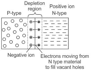
  • The depletion region/layer is an area at the junction where a field is formed because of the formation of a negative charge layer on the p side and a positive charge layer on the n side

Explanation:

  • The holes and electrons formed because of doping or impurities, diffuse to the other side respectively.
  • So when a hole diffuses across the junction, it leaves a negative donor ion and the electron leaves a positive charge on the n side.
  • These oppositely charged layers form a field due to the potential difference between the points which form the depletion region.
  • All of the stated points contribute to the formation of the depletion region at the junction. So option D is correct.
Test: The PN - Junction - Question 12

In forward bias, the width of potential barrier in a P-N junction diodIn forward bias, the width of potential barrier in a P-N junction diodee

Detailed Solution for Test: The PN - Junction - Question 12

Concept:
Forward Bias: 

  • When the negative terminal of the battery is connected to the N - side and the positive terminal to P - side the connection is called forward bias.


Explanation:

  • In forward biasing, the applied voltage V of the battery mostly drops across the depletion region and the voltage drops across the p-side and n-side of the p-n junction is negligibly small.
  • It is due to the fact that the resistance of the depletion region is very high as it has no free charge carriers.
  • In forward biasing the forward voltage opposes the potential barrier Vb. As a result of it, the potential barrier height is reduced and the width of the depletion layer decreases. Therefore option 2 is correct.
  • As forward voltage is increased, at a particular value the depletion region becomes very much narrow such that a large number of majority charge carriers can cross the junction.
Test: The PN - Junction - Question 13

For a reverse biased p-n junction:

Detailed Solution for Test: The PN - Junction - Question 13

Concept:

  • Diode: A diode is a two-terminal electronic component that conducts current primarily in one direction; it has low resistance in one direction, and high resistance in the other.

There are two 

  • Forward Biasing: 
    • The forward bias means the positive region is connected to the p-terminal of the supply and the negative region is connected to the n-terminal of the supply.
    • In forward biasing the external voltage is applied across the PN-junction diode. 
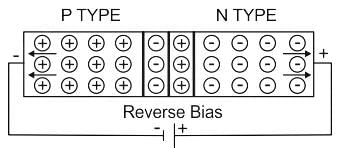
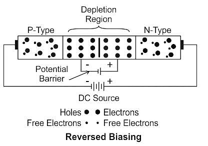
  • Reverse Biasing: 
    • ​In reversed bias, the negative region is connected to the positive terminal of the battery, and the positive region is connected to the negative terminal. ​
    • It creates a high resistive path in which no current flows through the circuit.

Explanation:

  • In reverse-biased the negative potential is applied to the P- region and a positive potential is applied to N - region.
  • Which attracts the electrons on the N- side towards the positive potential and the holes in the P - region is attracted to the negative potential applied on the P - region, which means the reverse current is produced due to the movement of both electrons and holes respectively.
  • Hence, option D is the answer
Test: The PN - Junction - Question 14

The increase in the width of the depletion region in a p-n junction diode is due to :

Detailed Solution for Test: The PN - Junction - Question 14

Concept:
Depletion region: 

  • The region near the p-n junction where the flow of charge carriers (free electrons and holes) is reduced over a given period and finally results in zero charge carriers.
  • The width of the depletion region depends on the number of impurities added to the semiconductor.

     
  • When a p-n junction is forward-biased:
    • The charge carriers are pushed towards the junction.
    • If the voltage of the battery is large enough diode-electrons reach the p-end and fill the holes.
    • So, The depletion layer is eliminated, and a current passes through the diode.
    • While the battery continues to supply electrons for the n-end, this removes electrons from the p-end, which works as supplying holes.
    • With a further increase in voltage from the battery, the current increases.

  • When a p-n junction is reverse biased:
    • Both the free electrons in the n-type semiconductor and the holes in the p-type semiconductor are attracted toward the battery.
    • The width of the depletion layer is increased, and no charge carriers meet.
    • Almost no current passes through the diode.
    • It acts like a very high ohm resistor or the same as an insulator. 

Explanation:

  • From the above explanation, we can see that, when a diode is forward-biased, then the depletion layer width decreases, and the barrier height is reduced which will leads to the conduction of electrons through the junction.
  • Similarly, when a diode is reverse biased, then the depletion layer width increases. Therefore option 4 is correct.
Test: The PN - Junction - Question 15

P-N junction diode works as insulator if connected:

Detailed Solution for Test: The PN - Junction - Question 15

Concept:

  • Diode: A diode is a two-terminal electronic component that conducts current primarily in one direction; it has low resistance in one direction, and high resistance in the other.

There are two 

  • Forward Biasing: 
    • The forward bias means the positive region is connected to the p-terminal of the supply and the negative region is connected to the n-terminal of the supply.
    • In forward biasing the external voltage is applied across the PN-junction diode. 
  • Reverse Biasing: 
    • ​In reversed bias, the negative region is connected to the positive terminal of the battery, and the positive region is connected to the negative terminal. ​
    • It creates a high resistive path in which no current flows through the circuit.

Explanation:


  • If a diode is reverse biased then the positive holes at the P-side of the junction are pulled toward the junction as negative potential is applied to the P- region.
  • Similarly, at the n -side of the junction, the electrons are pulled from the junction as positive potential is applied to n- region 
  • The width of the depletion layer increases. As the width of the depletion layer increases the amount of current-conducting is getting decreased.
  • Hence, if the diode is reverse biased then due to the increase in the width of the depletion layer the amount of current at the junction decreases and it acts as an insulator
  • Hence, option C is the answer
Test: The PN - Junction - Question 16

Which of the following formula represents the correct formula for width of the depletion region?

Detailed Solution for Test: The PN - Junction - Question 16

Correct formula for width of the depletion region is:

Test: The PN - Junction - Question 17

What is the maximum electric field when Vbi=2V , VR=5V and width of the semiconductor is 7cm?

Detailed Solution for Test: The PN - Junction - Question 17

Emax=-2(Vbi+VR)/W
=-2(2+5)/ (7*10-2)
=-200V/m.

Test: The PN - Junction - Question 18

During reverse bias, a small current develops known as

Detailed Solution for Test: The PN - Junction - Question 18

When the diode is reverse biased, a small current flows between the p-n junction which is of the order of the Pico ampere. This current is known as reverse saturation current.

Test: The PN - Junction - Question 19

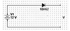
What will be the output of the following circuit? (Assume 0.7V drop across the diode)
Detailed Solution for Test: The PN - Junction - Question 19

V=12-0.7
=11.3V.

Test: The PN - Junction - Question 20

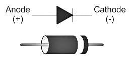
If the positive terminal of the battery is connected to the anode of the diode, then it is known as

Detailed Solution for Test: The PN - Junction - Question 20

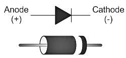
When a positive terminal is connected to the anode, the diode is forward biased which lets the flow of the current in the circuit.

25 docs|263 tests
Information about Test: The PN - Junction Page
In this test you can find the Exam questions for Test: The PN - Junction solved & explained in the simplest way possible. Besides giving Questions and answers for Test: The PN - Junction, EduRev gives you an ample number of Online tests for practice

Top Courses for Electronics and Communication Engineering (ECE)

Download as PDF

Top Courses for Electronics and Communication Engineering (ECE)