Electronics and Communication Engineering (ECE) Exam  >  Electronics and Communication Engineering (ECE) Tests  >  Electronic Devices  >  Practice Questions: Bipolar Junction Transistor (BJT) - 1 - Electronics and Communication Engineering (ECE) MCQ

Practice Questions: Bipolar Junction Transistor (BJT) - 1 - Electronics and Communication Engineering (ECE) MCQ


Test Description

10 Questions MCQ Test Electronic Devices - Practice Questions: Bipolar Junction Transistor (BJT) - 1

Practice Questions: Bipolar Junction Transistor (BJT) - 1 for Electronics and Communication Engineering (ECE) 2025 is part of Electronic Devices preparation. The Practice Questions: Bipolar Junction Transistor (BJT) - 1 questions and answers have been prepared according to the Electronics and Communication Engineering (ECE) exam syllabus.The Practice Questions: Bipolar Junction Transistor (BJT) - 1 MCQs are made for Electronics and Communication Engineering (ECE) 2025 Exam. Find important definitions, questions, notes, meanings, examples, exercises, MCQs and online tests for Practice Questions: Bipolar Junction Transistor (BJT) - 1 below.
Solutions of Practice Questions: Bipolar Junction Transistor (BJT) - 1 questions in English are available as part of our Electronic Devices for Electronics and Communication Engineering (ECE) & Practice Questions: Bipolar Junction Transistor (BJT) - 1 solutions in Hindi for Electronic Devices course. Download more important topics, notes, lectures and mock test series for Electronics and Communication Engineering (ECE) Exam by signing up for free. Attempt Practice Questions: Bipolar Junction Transistor (BJT) - 1 | 10 questions in 30 minutes | Mock test for Electronics and Communication Engineering (ECE) preparation | Free important questions MCQ to study Electronic Devices for Electronics and Communication Engineering (ECE) Exam | Download free PDF with solutions
Practice Questions: Bipolar Junction Transistor (BJT) - 1 - Question 1

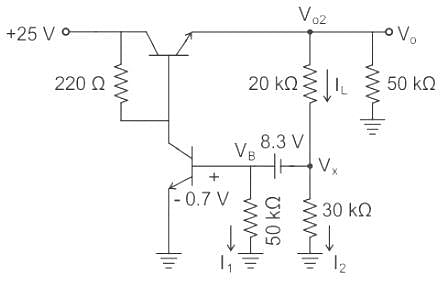
In the series voltage regulator circuit as given in below figure, VBE = 0.7 V, β = 50, VZ = 8.3 V. The output voltage V0 is:
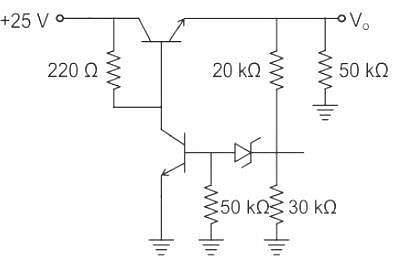
Detailed Solution for Practice Questions: Bipolar Junction Transistor (BJT) - 1 - Question 1

Redraw the circuit considering Zener diode operating at the breakdown region;


Practice Questions: Bipolar Junction Transistor (BJT) - 1 - Question 2

Considering adding impurities to semiconductors, what is the abbreviation for ‘ppm’?

Detailed Solution for Practice Questions: Bipolar Junction Transistor (BJT) - 1 - Question 2

Doping in semiconductor:

  • We usually add impurities to semiconductors, to increase their conductivity.
  • When a small amount say a few parts per million (ppm), of a suitable impurity is added to the pure semiconductor, the conductivity of the semiconductor is increased manifold.
  • The planned addition of a desirable impurity is called doping and the impurity atoms are called dopants.
  • The dopant has to be such that it does not distort the original pure semiconductor lattice.
  • It occupies only a very few of the original semiconductor atom sites in the crystal.
1 Crore+ students have signed up on EduRev. Have you? Download the App
Practice Questions: Bipolar Junction Transistor (BJT) - 1 - Question 3

Which of the following are the functions of a transistor?

Detailed Solution for Practice Questions: Bipolar Junction Transistor (BJT) - 1 - Question 3

Transistors:

  • Transistors are semiconductor devices, which are commonly used in amplifiers or electrically controlled switches
  • Transistors are the basic building block that regulates the operation of computers, mobile phones, and all the other modern electronic circuits
  • The most important transistor function is as a current amplifier and as a switch
  • Transistors as current amplifiers are often used in amplifiers while transistors as switches are often found in automatic light circuits
  • The functions of a transistor are variable resistor and switching device
Practice Questions: Bipolar Junction Transistor (BJT) - 1 - Question 4

A transistor connected in a common base configuration has the following readings IE = 2 mA and IB = 20 μA. Find the current gain α.

Detailed Solution for Practice Questions: Bipolar Junction Transistor (BJT) - 1 - Question 4

Current amplification factor: It is defined as the ratio of the output current to the input current. In the common-base configuration, the output current is emitter current IC, whereas the input current is base current IE.
Thus, the ratio of change in collector current to the change in the emitter current is known as the current amplification factor. It is expressed by the α.

Calculation:
Given,
IE = 2 mA
IB = 20 μA = 0.02 mA
From above concept,
IC = 2 mA - 0.02 mA = 1.98 mA
Current amplification factor is given as,

Practice Questions: Bipolar Junction Transistor (BJT) - 1 - Question 5

BJT is a _____

Detailed Solution for Practice Questions: Bipolar Junction Transistor (BJT) - 1 - Question 5

BJT stands for Bipolar junction transistor

  • B = Bipolar (because conduction is due to two opposite type of carriers Holes and electrons)
  • J = Junction refers to the two PN junctions between emitter and base, and collector and base.
  • BJT's are current-driven devices i.e. It is a current-controlled device.
  • The current through the two terminals is controlled by a current at the third terminal (base).
  • It is a bipolar device (current conduction by both types of carriers, i.e. majority and minority electrons and holes)
  • It has a low input impedance.

Symbol

Practice Questions: Bipolar Junction Transistor (BJT) - 1 - Question 6

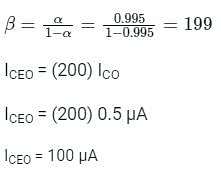
If α = 0.995, IE = 10 mA and ICO = 0.5 μA, then the value of ICEO is:

Detailed Solution for Practice Questions: Bipolar Junction Transistor (BJT) - 1 - Question 6

ICO = It is the reverse saturation current across reverse biased collector junction.

ICEO = Base cut-off current

ICEO = (1 +β) ICO

Practice Questions: Bipolar Junction Transistor (BJT) - 1 - Question 7

What is true with regard to the cut off region of npn BJT?

Detailed Solution for Practice Questions: Bipolar Junction Transistor (BJT) - 1 - Question 7

Consider a npn transistor

In cutoff region:
Collector base junction is reversed biased: VB < VC
Emitter base junction is reversed biased: VB < VE

In Saturation region:
Collector base junction is forward biased: VB > VC
Emitter base junction is forward biased: VB > VE

In Active region:
Collector base junction is reversed biased: VB < VC
Emitter base junction is forward biased: VB > VE

Practice Questions: Bipolar Junction Transistor (BJT) - 1 - Question 8

Four relations are given below. Identify the correct relation regarding a transistor.

Detailed Solution for Practice Questions: Bipolar Junction Transistor (BJT) - 1 - Question 8

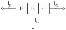
A transistor is a 3 layered 2 junction device as shown below.

IE = IB + IC
IC = βIB
IE > IC > IB

Practice Questions: Bipolar Junction Transistor (BJT) - 1 - Question 9

The built-in potential of a P N junction diode is 0.7 V at room temperature. What will be the approximate value of built-in potential if the doping concentrations on both sides are doubled?
Assume In (2) = 0.7

Detailed Solution for Practice Questions: Bipolar Junction Transistor (BJT) - 1 - Question 9

Concept:

  • As the N-type material has lost electrons and the P-type has lost holes, the N-type material has become positive with respect to the P-type.
  • Then the presence of impurity ions on both sides of the junction causes an electric field to be established across this region with the N-side at a positive voltage relative to the P-side.
  • The problem now is that a free charge requires some extra energy to overcome the barrier that now exists for it to be able to cross the depletion region junction.
  • This electric field created by the diffusion process has created a “built-in potential difference” across the junction with an open-circuit (zero bias) potential

Calculation:
Given built-in voltage of the diode is 0.7 V
Now doping concentrations on both sides are doubled. i.e, NA’ = 2NA and ND’ = 2ND
Newly built-in potential is:

Practice Questions: Bipolar Junction Transistor (BJT) - 1 - Question 10

A power transistor has:

Detailed Solution for Practice Questions: Bipolar Junction Transistor (BJT) - 1 - Question 10

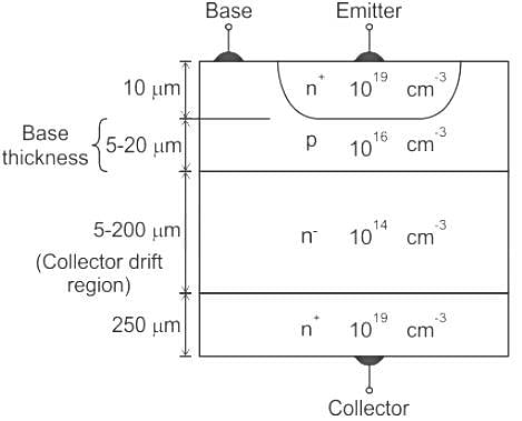
A power transistor is a three-terminal semiconductor electronic device
It has a four-layer structure of alternating P and N-type doping as shown below

  • The thickness of the drift region determines the breakdown voltage of the power transistor which is normally very high when compared to signal level transistors
  • This doping provides a capability to the transistors for higher current and higher voltage operability resulting in the application in high power application
21 docs|29 tests
Information about Practice Questions: Bipolar Junction Transistor (BJT) - 1 Page
In this test you can find the Exam questions for Practice Questions: Bipolar Junction Transistor (BJT) - 1 solved & explained in the simplest way possible. Besides giving Questions and answers for Practice Questions: Bipolar Junction Transistor (BJT) - 1, EduRev gives you an ample number of Online tests for practice

Top Courses for Electronics and Communication Engineering (ECE)

Download as PDF

Top Courses for Electronics and Communication Engineering (ECE)