Electronics and Communication Engineering (ECE) Exam  >  Electronics and Communication Engineering (ECE) Tests  >  Electronic Devices  >  Test: Common Collector Configuration - Electronics and Communication Engineering (ECE) MCQ

Test: Common Collector Configuration - Electronics and Communication Engineering (ECE) MCQ


Test Description

10 Questions MCQ Test Electronic Devices - Test: Common Collector Configuration

Test: Common Collector Configuration for Electronics and Communication Engineering (ECE) 2024 is part of Electronic Devices preparation. The Test: Common Collector Configuration questions and answers have been prepared according to the Electronics and Communication Engineering (ECE) exam syllabus.The Test: Common Collector Configuration MCQs are made for Electronics and Communication Engineering (ECE) 2024 Exam. Find important definitions, questions, notes, meanings, examples, exercises, MCQs and online tests for Test: Common Collector Configuration below.
Solutions of Test: Common Collector Configuration questions in English are available as part of our Electronic Devices for Electronics and Communication Engineering (ECE) & Test: Common Collector Configuration solutions in Hindi for Electronic Devices course. Download more important topics, notes, lectures and mock test series for Electronics and Communication Engineering (ECE) Exam by signing up for free. Attempt Test: Common Collector Configuration | 10 questions in 30 minutes | Mock test for Electronics and Communication Engineering (ECE) preparation | Free important questions MCQ to study Electronic Devices for Electronics and Communication Engineering (ECE) Exam | Download free PDF with solutions
Test: Common Collector Configuration - Question 1

Which amplifier circuit is used as an emitter follower circuit?

Detailed Solution for Test: Common Collector Configuration - Question 1
  • The common collector transistor circuit configuration gains its name from the fact that the collector circuit is common to both input and output circuits, the base is associated with only the input, and then the emitter with the output only.
  • The other name for the common collector is emitter follower. This name is derived from the fact that the emitter voltage "follows" that of the base circuit - the circuit has unit voltage gain.
  • The emitter follower transistor amplifier has a very straightforward circuit. The base is connected to the previous stage, and often this may be directly connected as this can save on additional bias resistors which lower the input impedance and hence increase the loading to the previous stage.


Test: Common Collector Configuration - Question 2

Identify the correct statement/s.
I. The other name for the common collector amplifier is emitter follower.
II. Power gain of the common emitter amplifier is high.

Detailed Solution for Test: Common Collector Configuration - Question 2
  • The common collector transistor circuit configuration gains its name from the fact that the collector circuit is common to both input and output circuits, the base is associated with only the input, and then the emitter with the output only.
  • The other name for the common collector is emitter follower. This name is derived from the fact that the emitter voltage "follows" that of the base circuit - the circuit has unit voltage gain.
  • The emitter follower transistor amplifier has a very straightforward circuit. The base is connected to the previous stage, and often this may be directly connected as this can save on additional bias resistors which lower the input impedance and hence increase the loading to the previous stage.
  • The power gain of a common emitter (CE) amplifier is higher than the power gain of a common collector (CC) amplifier or a common base (CB) amplifier


1 Crore+ students have signed up on EduRev. Have you? Download the App
Test: Common Collector Configuration - Question 3

Which one is suited best for impedance matching?

Detailed Solution for Test: Common Collector Configuration - Question 3
  • Common collector configuration, also known as emitter follower provides high input impedance and low output impedance. So they are used for the purpose of impedance matching.
  • In common collector configuration, the collector terminal is common to both input and output terminals. The current gain in the common-collector configuration is therefore the ratio of the emitter current to the base current.
  • Since the emitter current is very high as compared to the base current, we get current amplification.
  • It provides a voltage gain of less than unity.

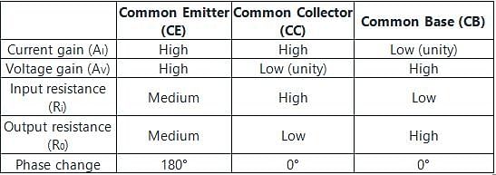
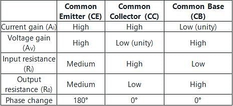
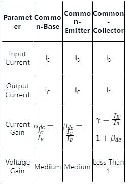
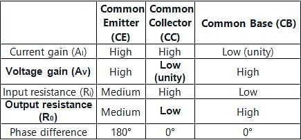
Important Differences between different transistor configuration is as shown:

Test: Common Collector Configuration - Question 4

Which of the following is NOT true for a common collector transistor?

Detailed Solution for Test: Common Collector Configuration - Question 4
  • The input impedance is high in the common collector because this is calculated by the Beta (gain) of the transistor, multiplied by the emitter resistance, whereas the current gain is due to the output impedance being inversely proportional to the current gain of the transistor in parallel to Re
  • Common collector configuration, also known as emitter follower provides high input impedance and low output impedance. So they are used for the purpose of impedance matching.
  • In common collector configuration, the collector terminal is common to both input and output terminals. The current gain in the common-collector configuration is therefore the ratio of the emitter current to the base current. Since the emitter current is very high as compared to the base current, we get current amplification. It provides a voltage gain of less than unity.

common collector configuration has low voltage gain and high current gain. The power gain of the common collector amplifier is medium. so option 4 is wrong

Test: Common Collector Configuration - Question 5

The output signal of a common-collector amplifier is always:-

Detailed Solution for Test: Common Collector Configuration - Question 5

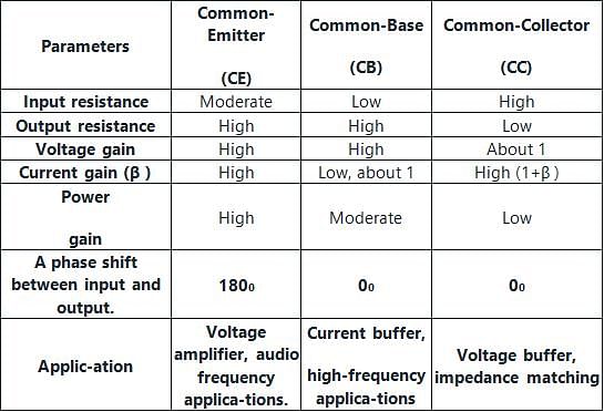
All the configurations are used in different circuits based on their applications:

Test: Common Collector Configuration - Question 6

The phase shift between input and output of an emitter follower is _____

Detailed Solution for Test: Common Collector Configuration - Question 6

The phase shift between the input and output of an emitter follower is 0º.
Emitter follower:

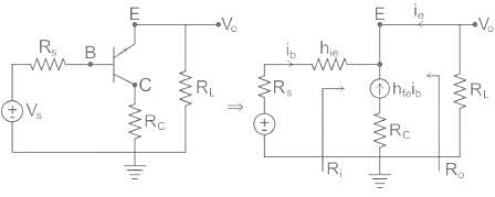
  • The Emitter-follower circuit is also known as a common collector configuration.
  • It is called the emitter follower configuration because the emitter voltage follows the base voltage.
  • It is mostly used as a voltage buffer.
  • The small-signal model & hybrid model is shown below:

Test: Common Collector Configuration - Question 7

The output and input voltages of an emitter-follower have a phase difference of _______.

Detailed Solution for Test: Common Collector Configuration - Question 7

The phase shift between the input and output of an emitter follower is 0º.
Emitter follower:

  • The Emitter-follower circuit is also known as a common collector configuration.
  • It is called the emitter follower configuration because the emitter voltage follows the base voltage.
  • It is mostly used as a voltage buffer.
  • The small-signal model & hybrid model is shown below:

Test: Common Collector Configuration - Question 8

A buffer is:

Detailed Solution for Test: Common Collector Configuration - Question 8

Buffer:

  • A Buffer is an op-amp circuit whose output voltage straight away follows the input voltage. i.e. output voltage equivalent to the input voltage.
  • The Op-amp circuit does not provide any amplification thus, its voltage gain is unity.
  • The voltage follower is used as a buffer amplifier, isolation amplifier, unity gain amplifier as the output follows the input.
  • The voltage follower provides no alternation or amplification but only buffering.


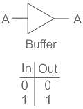
Non-Inverting Buffer:
1. The buffer is a single-input device that has a gain of 1and provides the input at the output.
2. It has value for impedance matching and for isolation of the input and output.

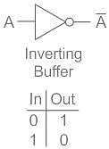
Inverting Buffer:
1. The inverting buffer is a single-input device that produces the state opposite the input.
2. If the input is high, the output is low and vice versa.

Hence option (2) is the correct answer.
Characteristics:

  • High input impedance
  • Low output impedance
  • Current Gain & power gain high
  • Voltage gain unity
Test: Common Collector Configuration - Question 9

A voltage buffer has the following characteristics:

Detailed Solution for Test: Common Collector Configuration - Question 9

Common Collector configuration is also known as voltage buffer and emitter follower as it has unity voltage gain.

  • CB configuration: Low Input impedance and High output impedance
  • CC configuration: (Emitter follower): High Input impedance and low output impedance
  • CE configuration: Moderate Input impedance and Moderate output impedance

Test: Common Collector Configuration - Question 10

The output impedance of a BJT under common-collector configuration is

Detailed Solution for Test: Common Collector Configuration - Question 10
  • Common collector configuration, also known as emitter follower provides high input impedance and low output impedance. So they are used for the purpose of impedance matching.
  • In common collector configuration, the collector terminal is common to both input and output terminals.

Important Differences between different transistor configuration is as shown:

21 docs|29 tests
Information about Test: Common Collector Configuration Page
In this test you can find the Exam questions for Test: Common Collector Configuration solved & explained in the simplest way possible. Besides giving Questions and answers for Test: Common Collector Configuration, EduRev gives you an ample number of Online tests for practice

Top Courses for Electronics and Communication Engineering (ECE)

Download as PDF

Top Courses for Electronics and Communication Engineering (ECE)