Physics Exam  >  Physics Tests  >  GATE Physics Mock Test Series 2025  >  Test: Electronics - 2 - Physics MCQ

Test: Electronics - 2 - Physics MCQ


Test Description

20 Questions MCQ Test GATE Physics Mock Test Series 2025 - Test: Electronics - 2

Test: Electronics - 2 for Physics 2024 is part of GATE Physics Mock Test Series 2025 preparation. The Test: Electronics - 2 questions and answers have been prepared according to the Physics exam syllabus.The Test: Electronics - 2 MCQs are made for Physics 2024 Exam. Find important definitions, questions, notes, meanings, examples, exercises, MCQs and online tests for Test: Electronics - 2 below.
Solutions of Test: Electronics - 2 questions in English are available as part of our GATE Physics Mock Test Series 2025 for Physics & Test: Electronics - 2 solutions in Hindi for GATE Physics Mock Test Series 2025 course. Download more important topics, notes, lectures and mock test series for Physics Exam by signing up for free. Attempt Test: Electronics - 2 | 20 questions in 40 minutes | Mock test for Physics preparation | Free important questions MCQ to study GATE Physics Mock Test Series 2025 for Physics Exam | Download free PDF with solutions
*Answer can only contain numeric values
Test: Electronics - 2 - Question 1

Number of comparators required to build a 5-bit analog to digital convertor (ADC) is__________(your answer should be an integers)


Detailed Solution for Test: Electronics - 2 - Question 1

For "n’ bit number of comparators = 2n - 1
So for ‘5 ' bits =  25 - 1 = 31

Test: Electronics - 2 - Question 2

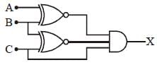
For logic circuit shown, the required inputs A, B and C to make the output X = 1 are respectively.

Detailed Solution for Test: Electronics - 2 - Question 2

Here, output X = 
For XNOR operation when both input same then output will be high.
So, X = 
X = 
So for desired output X = 1 input A, B, C must be high.

1 Crore+ students have signed up on EduRev. Have you? Download the App
Test: Electronics - 2 - Question 3

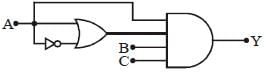
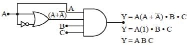
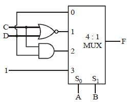
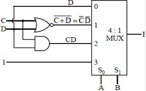
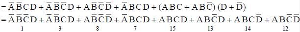
The Boolean expression for the output Y in the logic circuit is

Detailed Solution for Test: Electronics - 2 - Question 3

Test: Electronics - 2 - Question 4

Refer to figure shown below:

Detailed Solution for Test: Electronics - 2 - Question 4

When Vi > 0 then op-amp will give negative output, because it is applied at inverting terminal.
So diode (Di) is F.B. and diode D2 is R.B. because V'0 will be negative.
When D2 OFF so V0 = 0
Note : There is no need to check V< 0 

Test: Electronics - 2 - Question 5

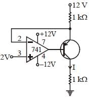
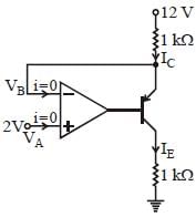
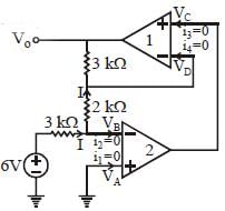
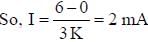
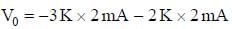
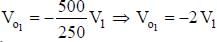
An op-anip circuit is shown in given figure. The current I is ?

Detailed Solution for Test: Electronics - 2 - Question 5

As Ideal op-amp lias infinite input resistance so there will be no current pass through op-amp VA and VB will be virtual ground VB = VA = 2 V .

So, 
So, I = 10 mA

*Answer can only contain numeric values
Test: Electronics - 2 - Question 6

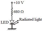
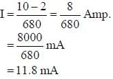
The light emitting diode (LED), shown in the above figure has a voltage drop of 2V. The current flowing through LED is_____________mA (your answer should be first decimal place)


Detailed Solution for Test: Electronics - 2 - Question 6

LED diodes works in forward bias.
The current flowing though LED is

Test: Electronics - 2 - Question 7

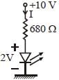
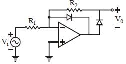
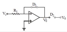
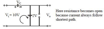
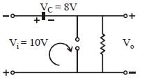
Select the coll ect output (Vo) wave-shape for a given input (Vi) in the clamping network given below:

Detailed Solution for Test: Electronics - 2 - Question 7

It is a simple clamper circuit in which the diode is downward direction. So the total signal will be clamp below the reference voltage (2V).
Alternate Method :
When positive terminal of input voltage Vi = +10 V , diode is F.B.
Therefore, Vo = 2V
Apply KVL at the loop.
V- V- v= 0
10 - VC -2 = 0
V= 8V

When negative tenninal of input voltage Vi = -10 V . Diode is reverse biased. Apply KVL at the given loop.
Vi - V- V= 0
-10-8 = Vo
∴ Vo= -18V


Test: Electronics - 2 - Question 8

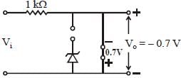
In the following limiter circuit an input voltage Vi =10 sin 100 πt is applied. Assume that the diode drop is 0.7V when it is F.B. The zener break down voltage is 6.8 V.

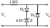
The maximum and minimum values of the output voltage respectively are :

Detailed Solution for Test: Electronics - 2 - Question 8

For the positive half cycle of V, D1 is forward biased and zener diode is in break down stage.
So, Vo= 0.7 + 6.8 = 7.5 V
For the negative half cycle of Vi,D2 is forward biased.
So V0 = -0.7 V.

Test: Electronics - 2 - Question 9

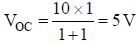
In the circuit shown below, the zener diode is ideal and zener voltage is 6V. The output voltage Vo (in volts) is

Detailed Solution for Test: Electronics - 2 - Question 9

Firstly check the zener diode is conducting or not conducting. To check this O.C. the Z.D. and calculate open circuit voltage (VOC )
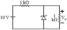
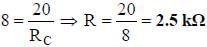
 By voltage divider rule.
Here, VOC < VZ , so Z.D. is not conducting.
Then, Vo = VOC = 5 V

Test: Electronics - 2 - Question 10

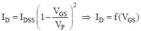
In n-channel depletion type MOSFET when drain terminal is positive biased w.r.t. source and if VGS is applied with negative voltage on the gate terminal, then what will be done ?

Detailed Solution for Test: Electronics - 2 - Question 10

When VGS is applied gate is given with negative voltage and therefore positive charges are created in the semi-conductor channel and due to the recombination less no of negative charges or electrons will reaching the drain. Therefore, drain current (ld) decreases.

Test: Electronics - 2 - Question 11

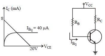
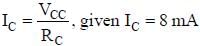
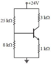
Given the device characteristics of figure, determine Vcc and Rc for fixed bia s configuration ?

Detailed Solution for Test: Electronics - 2 - Question 11

Apply KVL for emitter-collector loop
VCC = ICRC + VCE
when IC = 0, VCE = VCC ⇒ VCC = 20 V
IC RC = VCC - VCE when VCE = 0


Test: Electronics - 2 - Question 12

Match the following ?

Detailed Solution for Test: Electronics - 2 - Question 12

(i) FET is voltage control current source as

(ii) Op-Any. is voltage control voltage source
Output voltage o f op-amp Vat inverting terminal
V0 ∝ f (Vi)
(iii) BJT current control current source as
I= β I⇒ I= f  (Ib)

Test: Electronics - 2 - Question 13

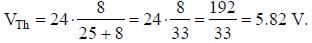
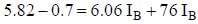
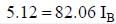
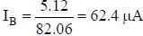
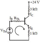
For the circuit shown below, let β = 75 . The Q-point (ICQ - VCEQ) is


Detailed Solution for Test: Electronics - 2 - Question 13

The given circuit can be convert in to Tkevenin’s equivalent circuit.


Applying KVL at base-emitter loop.


Test: Electronics - 2 - Question 14

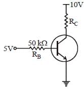
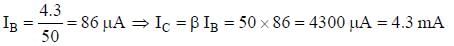
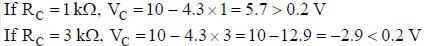
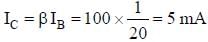
In the circuit shown, the silicon BJT has β = 50. Assume VBE = 0 .7 V and VCE(sat) =   0.2V, which one of the following statements is correct ?

Detailed Solution for Test: Electronics - 2 - Question 14

Here the base emitter junction is forward bias so there is no chance in cut-off mode of given transistor.
Assume transistor in active mode.
Apply KVL at base-emitter loop.

If VCE < 0 .2 V, then transistor in saturation.
To check the mode by putting the value RC in the given option.

So transistor in saturation at RC = 3 kΩ

Test: Electronics - 2 - Question 15

The boolean function realized by the following circuit is

Detailed Solution for Test: Electronics - 2 - Question 15

MUX output


Test: Electronics - 2 - Question 16

The circuit shown below the value of V0 is

Detailed Solution for Test: Electronics - 2 - Question 16


Since, ideal op-amp lias infinite input resistance so there will be no current pass through the op-amp.
So, VA = VB and Vc = VD due to virtual ground concept.
V= V= 0


= -6 -4
=-10 V

Test: Electronics - 2 - Question 17

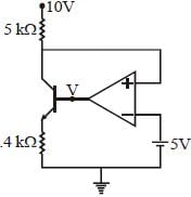
In the circuit shown below, the op-amp is ideal, the transistor has VBE = 0.6 V and β = 150. Decide whether the feedback in the circuit is positive or negative and determine the voltage V at the output of op-amp.
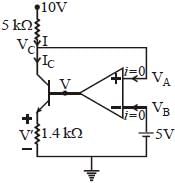
Detailed Solution for Test: Electronics - 2 - Question 17

Voltage at inverting terminal VB = 5 V. Ideal op-amp has infinite input resistance so there will be no current pass through the op-amp. So VA and VB will be virtual grounded, VA = VB =5V.

Since, VC = VA = 5 V

Here given p is very large, so IC  IE = 1 mA
V' = 1.4 x 103 x 1 x 10-3  = 1.4 V
Therefore, output voltage V = V' + VBE =1.4 + 0.6 = 2V
There is no need to check positive or negative feedback because 2V is available only in option (d).

Test: Electronics - 2 - Question 18

Determine the output voltage

Detailed Solution for Test: Electronics - 2 - Question 18

As the ideal op-amp has infinite input resistance so there will be no current pass through op-amp. In the given circuit the input voltage is applied at inverting terminal so it is work as inverting amplifier.
So output for first op-amp 
Similarly, output for second op-amp

*Answer can only contain numeric values
Test: Electronics - 2 - Question 19

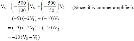
Ill the circuit shown, assume that the diodes D1 and D2 are ideal. The average value of voltage Vab(in volts),
across terminal 'a’ and 'b' is__________V (your answer should be an integer)


Detailed Solution for Test: Electronics - 2 - Question 19

Case-I : When input is positive D1 is ON and D2 is OFF. Tlien equivalent circuit is

Case-II : When input is negative D1 if OFF and D2 is ON.

(By applying voltage divider rule).

Thus the average value of Vab = 5 V.

*Answer can only contain numeric values
Test: Electronics - 2 - Question 20

In the circuit shown.

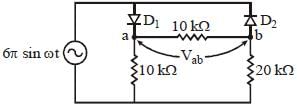
The transistor is biased at___________mA (your answer should be upto first decimal place)


Detailed Solution for Test: Electronics - 2 - Question 20

Since, emitter junction is F.B. So BJT is not in cut-offmode. It maybe either active or saturation region.
Let us assume transistor in active region.
Then, applying KVL at base-emitter loop.
2.7 - 40 K IB -0.7 = 0
40 K IB = 2
IB = 0.05 mA

Applying KVL at emitter collector loop.


Since, VCE < 0.5, so transistor is not in active region it is saturation region.

1 docs|34 tests
Information about Test: Electronics - 2 Page
In this test you can find the Exam questions for Test: Electronics - 2 solved & explained in the simplest way possible. Besides giving Questions and answers for Test: Electronics - 2, EduRev gives you an ample number of Online tests for practice
Download as PDF