Analog Electronics - 3 - Free MCQ Test with solutions for GATE EE and Digital
MCQ Practice Test & Solutions: Analog Electronics - 3 (10 Questions)
You can prepare effectively for Electrical Engineering (EE) Analog and Digital Electronics with this dedicated MCQ Practice Test (available with solutions) on the important topic of "Analog Electronics - 3". These 10 questions have been designed by the experts with the latest curriculum of Electrical Engineering (EE) 2026, to help you master the concept.
Test Highlights:
- - Format: Multiple Choice Questions (MCQ)
- - Duration: 30 minutes
- - Number of Questions: 10
Sign up on EduRev for free to attempt this test and track your preparation progress.

When the gate-to-source voltage VGS of a MOSFET with a threshold voltage of 400mV, working in saturation is 900mV, the drain current is observed to be 1mA. Neglecting the channel width modulation effect and assuming that the MOSFET is operating at saturation, the drain current for an applied VGS of 1400mV is
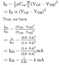
Detailed Solution: Question 1
What percentage of current IDSS is the drain current for a JFET, if the gate to source voltage is 65% of the pinch-off voltage.
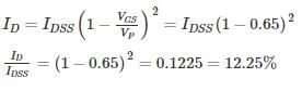
Detailed Solution: Question 2

The ‘Pinch-off’ voltage of a JFET is 4 V. Then the off gate voltage of JFET is
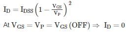
Detailed Solution: Question 3
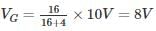
A MOSFET operating in saturation mode is shown in the below figure. The drain current is given as ID = ½ (VGS – 0.75)2 mA If VS = 5V, then the value of RS in kΩ is __________
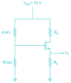
Detailed Solution: Question 4
For the amplifier shown below, the drain current changes from 5 mA to 7 mA when the gate voltage D changed from -4.0 V to -3.7 V. The voltage gain of the amplifier is _____
Detailed Solution: Question 5

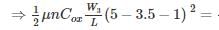
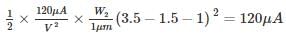
The NMOS transistors in the circuit below have VT = 1 V, μncox = 120 μA/V2, λ = 0 and L1 = L2 = L3 = 1 μm. The values of width of each of Q1, Q2, Q3 such that the voltage values are as shown in below figure are
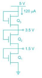
Detailed Solution: Question 6


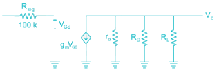
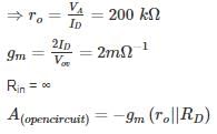
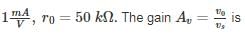
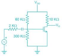
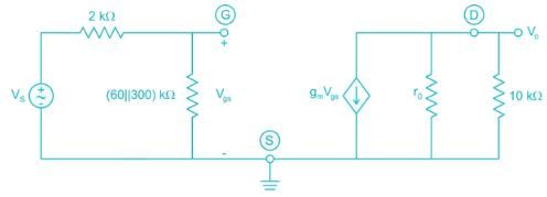
A common source amplifier biased at ID = 0.25 mA with RD = 20 kΩ and early voltage VA = 50 V and overdrive voltage (VGS – VT)DC = 0.25 V. If the input is fed through 100 kΩ and output are taken from 20 kΩ loads then the overall gain of the amplifier is _____ V/V.
Detailed Solution: Question 7
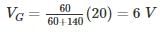
The transistor I the circuit is shown below has parameters IDSS = 8 mA and VP = -4 V. The value of VDS is___
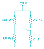
Detailed Solution: Question 8
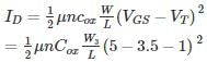
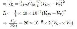
The small signal resistance (dVC/dID) of the n-channel MOSFET shown in figure below at bias voltage VC = 2V is (in kΩ) _________
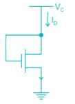
Given μnCox W/L = 40μ A/V2
VT = 1 V
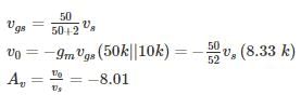
Detailed Solution: Question 9

Detailed Solution: Question 10
135 videos|183 docs|71 tests |