Test: Electronic Devices - 3 - Electronics and Communication Engineering (ECE) MCQ
10 Questions MCQ Test GATE ECE (Electronics) Mock Test Series 2025 - Test: Electronic Devices - 3

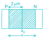
The open-circuit p-n junction diode without any Biasing is shown if NA = 2 × 10¹⁷/cm3, ND = 5 × 10¹⁶/cm3 then the depletion region width (W) is ______μm
For the diode circuit shown below, If Vs = 24 sin 100πt, and the diode is practical with a cut in voltage of 0.7 V. The conduction angle of the circuit is _______ Degrees.

| 1 Crore+ students have signed up on EduRev. Have you? Download the App |
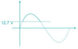
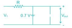
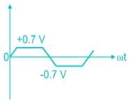
The correct output waveform for the circuit shown if the input is a sinusoidal signal of maximum Amplitude Vmax is
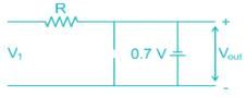
The correct output waveform for the circuit shown if the input is a sinusoidal signal of maximum Amplitude Vmax is
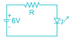
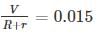
In the circuit shown, the forward biased LED has a voltage drop of 1.5 volts. If the battery voltage is 6V. Then the power displaced in the resistor R in milliwatts is _________mW. Current through LED is 15mA.
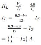
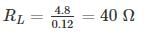
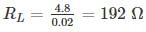
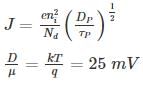
The voltage regulator circuit using a Zener diode is shown. The Zener diode current is limited in the range 5 ≤ iz ≤ 100 mA
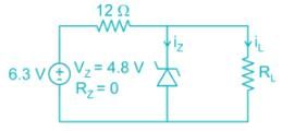
The range of load resistance is
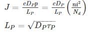
For a P±n Si junction the reverse current at room temperature is 0.9 nA/cm2. If donor density is 1015 cm-3 and intrinsic carrier concentration is 1.05 × 10¹⁰. The minority carrier life time is ________ n sec.
[Assume μP = 450 cm2/V-sec, kT = 25mV ]
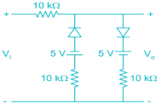
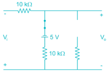
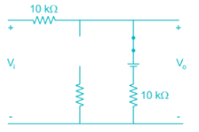
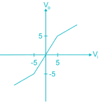
The sketch of output voltage Vo vs. input voltage VI is of from
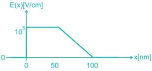
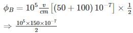
Consider a pn junction at zero bias with an electric distribution as sketched below. Calculate the built-in-potential
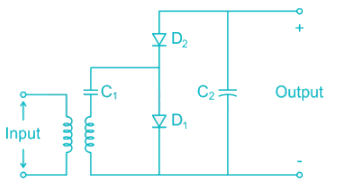
The correct waveform of the output of the given circuit is
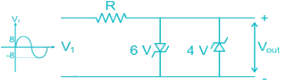
Assume the Zener diodes are ideal with threshold voltage Vk = 0.7
The correct statement regarding depletion and diffusion capacitance is
i) Depletion capacitance is dominant in reverse-bias voltage
ii) Diffusion capacitance is dominant in reverse-bias voltage
iii) The diffusion capacitance is due to a stored charge of minority electrons and minority holes near the depletion region
iv) Depletion capacitance is directly proportional to the width of the depletion region
|
25 docs|263 tests
|
|
25 docs|263 tests
|
Top Courses for Electronics and Communication Engineering (ECE)


Important Questions for Electronic Devices - 3
Electronic Devices - 3 MCQs with Answers
Online Tests for Electronic Devices - 3 GATE ECE (Electronics) Mock Test Series 2025
|
© EduRev
|
Education Revolution
|


|


