Test: Electronic Devices - 5 - Electronics and Communication Engineering (ECE) MCQ
10 Questions MCQ Test GATE ECE (Electronics) Mock Test Series 2025 - Test: Electronic Devices - 5

The figure shows the VTC characteristics of an NMOS inverter with three varying resistive loads (R).
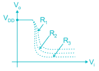
The correct statement is:
The correct statement is:
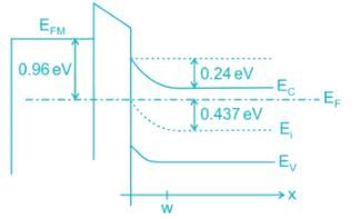
Assume that the zero for electrostatic potential is in the semiconductor bulk at large x and that there is no metal semiconductor work function difference. The relative dielectric constant for the oxide is ϵr = 11.8. If the intrinsic concentration is 1010/cm3. The doping density ND is _____ × 1017/cm3 (KT = 0.026 V)
| 1 Crore+ students have signed up on EduRev. Have you? Download the App |
The figure shows MOS capacitor variation with applied gate voltage for n-type body/substrate.
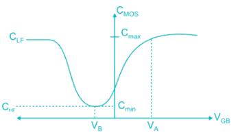
The flat band voltage is:
The flat band voltage is:
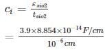
The insulator capacitance Ci of an ideal MOS capacitor with 10-nm gate oxide (εr = 3.9) on p-type Si with Na = 1016 cm-3 is ________ × 10-7 F/cm2
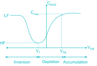
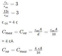
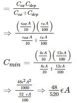
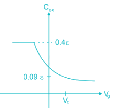
Which of the following curves represents the correct C – V characteristics of an NMOS transistor having an oxide layer thickness of 10 nm and a maximum depletion thickness of 100 nm. [Assume ϵs = permittivity of semiconductor, ϵox = permittivity of oxide and 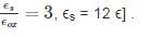
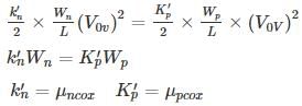
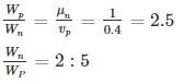
The mobility of hole is 0.4 times the mobility of electron. What must be the ratio of width of n-channel to p-channel MOSFET if they are to have equal drain currents when operated in saturation mode with same magnitude of overdrive voltage:
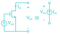
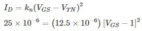
The circuit shown uses an NMOS transistor to implement a current source. For the transistor VTN = 1V and  =12.5 uA/V2. The required value of VGS to get IDC = 25 μA and corresponding compliance voltage is:
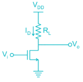
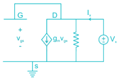
The output resistance R0 of the NMOS circuit if ID = 0.5 mA, λ = 0.02 V-1,  _____ kilo ohms.


For a MOSFET with gate plate area 0.5 × 10⁻² cm2 and oxide layer thickness 80 nm, the value of MOS capacitance and its break down voltage are: (assume relative di-electric constant of sio2, ϵr = 4 and ϵ0 = 8.854 × 10⁻¹⁴ F/cm and dielectric strength of sio2 film is 5 × 10⁶ V/cm)

 greater than dielectric strength (5 × 10⁶ V/cm)
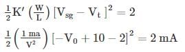
In the circuit shown in Figure, Transistors are characterized by 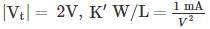 and λ = 0
The output voltage V0 is _______V
|
25 docs|263 tests
|
|
25 docs|263 tests
|
Top Courses for Electronics and Communication Engineering (ECE)


Important Questions for Electronic Devices - 5
Electronic Devices - 5 MCQs with Answers
Online Tests for Electronic Devices - 5 GATE ECE (Electronics) Mock Test Series 2025
|
© EduRev
|
Education Revolution
|


|


