Test: Electronic Devices - 6 - Electronics and Communication Engineering (ECE) MCQ
10 Questions MCQ Test GATE ECE (Electronics) Mock Test Series 2025 - Test: Electronic Devices - 6

The finer resolution in lithography can be obtained using
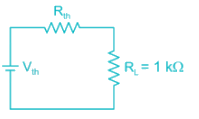
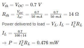
An ideal solar cell has a short-circuit current of 50 mA and an open circuit voltage of 0.7 V under full illumination. The power delivered to a load of 1 kΩ is ________ mW
| 1 Crore+ students have signed up on EduRev. Have you? Download the App |
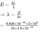
The wavelength of the emitted radiation by an electron while transferring from one energy state of -15eV to other states of -5eV is approximately(in nanometer)
A solar cell has a short circuit current of 10 mA and open circuit voltage of 0.9 V. The maximum power delivered by the solar cell is _________ mV. Given fill factor as 0.8.
The smallest feature that can be printed with adequate control using photolithography in controlled by
(a) The smallest image that can be projected on the wafer
(b) Resolving capability of photoresist
(c) Temperature of wafer
(d) The energy of Ion Implantation beam.
The correct statement is

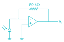
A photo – detector circuit is given in the figure. The photo diode has an active area of 10-2 cm2 and sensitivity of 0.65 A/w. When light of intensity 20 mW/cm2 falls on the photo diode, the output Vo is _______
Consider the following statements about thermal diffusion of dopants in IC fabrication.
a) Thermal diffusion should be carried out at later stages of the IC fabrication process
b) The lithographic mask used for diffusion should be of hard masks like oxide or nitride
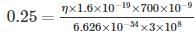
A photo diode is illuminated by light with 700 nm wavelength and power of 4 mW. If the open circuit current produced is 1mA then the internal quantum efficiency of photo diode is

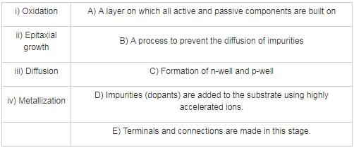
Match th4e various process in CMOS fabrication with appropriate description in second list
A Ga – As LED has a refractive index of 3.6 and is surrounded by air (μ = 1). If the bandgap of Ga – As is 1.43. Then out of 500 photons generated in Ga – As The number of photons emitted out of the specimen are _____

|
25 docs|263 tests
|
|
25 docs|263 tests
|
Top Courses for Electronics and Communication Engineering (ECE)


Important Questions for Electronic Devices - 6
Electronic Devices - 6 MCQs with Answers
Online Tests for Electronic Devices - 6 GATE ECE (Electronics) Mock Test Series 2025
|
© EduRev
|
Education Revolution
|


|


