Test: The Bipolar Junction Transistor - Electronics and Communication Engineering (ECE) MCQ
20 Questions MCQ Test GATE ECE (Electronics) Mock Test Series 2025 - Test: The Bipolar Junction Transistor
A uniformly doped silicon pnp transistor is biased in the forward-active mode. The doping profile is NE = 108 cm-3, NB = 5.2 x 1016 cm-3 and NC = 1015 cm-3 .For VEB = 0.6 V, the pB at x =0 is
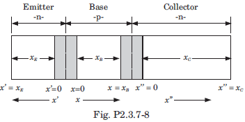
An npn bipolar transistor having uniform doping of NE = 1018 cm-3 NB = 1016 cm-3 and Nc = 6 x 1015 cm-3 is operating in the inverse-active mode with VBE = - 2 V and VBC = 0.6 V. The geometry of transistor is shown in fig
Q. The minority carrier concentration at x = xB is
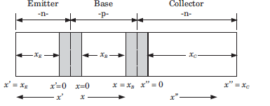
An npn bipolar transistor having uniform doping of NE = 1018 cm-3 NB = 1016 cm-3 and Nc = 6 x 1015 cm-3 is operating in the inverse-active mode with VBE = - 2 V and VBC = 0.6 V. The geometry of transistor is shown in fig

Q. The minority carrier concentration at x" = 0 is
An pnp bipolar transistor has uniform doping of NE = 6 x 1017 cm-3, NB = 2 x 1016 cm-3 and NC = 5 x 1014 cm-3. The transistor is operating is inverse-active mode. The maximum VCB voltage, so that the low injection condition applies, is
The following currents are measured in a uniformly doped npn bipolar transistor:
InE = 1.20 mA, IpE = 0.10 mA, InC = 1.18 mA
IR = 0.20 mA, IG = 1 μA, IpC0 = 1 μA
Q.
The α is
The following currents are measured in a uniformly doped npn bipolar transistor:
InE = 1.20 mA, IpE = 0.10 mA, InC = 1.18 mA
IR = 0.20 mA, IG = 1 μA, IpC0 = 1 μA
Q.
The β is
The following currents are measured in a uniformly doped npn bipolar transistor:
InE = 1.20 mA, IpE = 0.10 mA, InC = 1.18 mA
IR = 0.20 mA, IG = 1 μA, IpC0 = 1 μA
Q.
The γ is
A silicon npn bipolar transistor has doping concentration of NE = 2 x 1018cm-3, NB =1017cm-3 and NC = 15 x 1016 cm-3. The area is 10-3 cm2 and neutral base width is 1 μm. The transistor is biased in the active region at VBE = 0.5 V. The collector current is
(DB = 20 cm2/s)
A uniformly doped npn bipolar transistor has following parameters:
NE = 1018 cm-3 NB = 5 x 1016 cm-3,
Nc = 2 x 1019 cm-3,
DE = 8 cm2 /s , DB = 15 cm2 /s , Dc = 14 cm2 /s
xE = 0.8 μm, xB = 0.7 μm
The emitter injection efficiency γ is
In bipolar transistor biased in the forward-active region the base current is IB = 50 μA. and the collector currents is IC = 27 μA. The α is
For the transistor in fig., IS = 1015 A, βF = 100, βR = 1. The current ICBO is
Determine the region of operation for the transistor shown in circuit in question
Determine the region of operation for the transistor shown in circuit in question
Determine the region of operation for the transistor shown in circuit in question.
Determine the region of operation for the transistor shown in circuit in question.
For the circuit shown in fig., let the value of βR =0.5 and βF = 50. The saturation current is 10-16 A
Q. The base-emitter voltage is
For the circuit shown in fig., let the value of βR =0.5 and βF = 50. The saturation current is 10-16 A
Q. The current I1 is
The leakage current of a transistor are ICBO = 5μA and ICEO = 0.4 mA, and IB =30 μA
Q. The value of β is
The leakage current of a transistor are ICBO = 5μA and ICEO = 0.4 mA, and IB =30 μA
Q. The value of IC is
For a BJT, IC = 5 mA, IB = 50 μA and ICBO = 0.5μA.
Q. The value of β is
|
25 docs|263 tests
|


 = 0
= 0