Electronics and Communication Engineering (ECE) Exam  >  Electronics and Communication Engineering (ECE) Tests  >  GATE ECE (Electronics) Mock Test Series 2025  >  Analog Electronics - 2 - Electronics and Communication Engineering (ECE) MCQ

Analog Electronics - 2 - Electronics and Communication Engineering (ECE) MCQ


Test Description

10 Questions MCQ Test GATE ECE (Electronics) Mock Test Series 2025 - Analog Electronics - 2

Analog Electronics - 2 for Electronics and Communication Engineering (ECE) 2025 is part of GATE ECE (Electronics) Mock Test Series 2025 preparation. The Analog Electronics - 2 questions and answers have been prepared according to the Electronics and Communication Engineering (ECE) exam syllabus.The Analog Electronics - 2 MCQs are made for Electronics and Communication Engineering (ECE) 2025 Exam. Find important definitions, questions, notes, meanings, examples, exercises, MCQs and online tests for Analog Electronics - 2 below.
Solutions of Analog Electronics - 2 questions in English are available as part of our GATE ECE (Electronics) Mock Test Series 2025 for Electronics and Communication Engineering (ECE) & Analog Electronics - 2 solutions in Hindi for GATE ECE (Electronics) Mock Test Series 2025 course. Download more important topics, notes, lectures and mock test series for Electronics and Communication Engineering (ECE) Exam by signing up for free. Attempt Analog Electronics - 2 | 10 questions in 30 minutes | Mock test for Electronics and Communication Engineering (ECE) preparation | Free important questions MCQ to study GATE ECE (Electronics) Mock Test Series 2025 for Electronics and Communication Engineering (ECE) Exam | Download free PDF with solutions
Analog Electronics - 2 - Question 1

For the transistor circuit shown below:
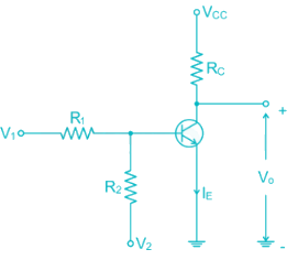
If V1 = 1V and V2 = -12V R1 = 15k and R2 = 100k R= 2.2 k Vcc = 12V Then the Region of operation of transistor is 

Detailed Solution for Analog Electronics - 2 - Question 1

V1 = 1V

V2 = -12V

R1 = 15 k

R2 = 100 k

= -0.7V

VBB­ < 0, the Base emitter Junction is reversed biased

Hence Transistor is in cut off mode

*Answer can only contain numeric values
Analog Electronics - 2 - Question 2

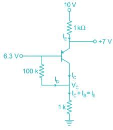
Calculate the value of β for the following circuit


Detailed Solution for Analog Electronics - 2 - Question 2


I= (1 + β) Iβ

3 × 10-3 = (1 + β) × 0.33 × 10⁻³

β = 89.9

1 Crore+ students have signed up on EduRev. Have you? Download the App
Analog Electronics - 2 - Question 3

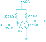
In the DC fixed bias circuit shown below the operating point is
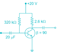
Detailed Solution for Analog Electronics - 2 - Question 3


So the operating point is (5.43 mA, 5.89 V)

Analog Electronics - 2 - Question 4

The Miller effect in the context of a Common Emitter amplifier explains

Detailed Solution for Analog Electronics - 2 - Question 4

The miller effect causes increase in the Input capacitance increase in the Input capacitance of Common – Emitter Amplifier

Upper cutoff frequency 

Therefore, there is decrease in upper-cut off frequency & Bandwidth of CE Amplifier

*Answer can only contain numeric values
Analog Electronics - 2 - Question 5

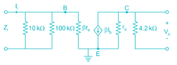
For the network shown in the figure. Find the Input independence Zi (kΩ) [Use appropriate approximation]
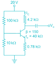

Detailed Solution for Analog Electronics - 2 - Question 5

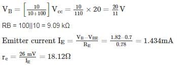
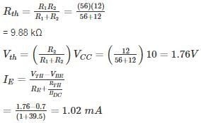
DC analysis from voltage divider

Now using appropriate approximations.

Z ≅ βre = 150 × 18.2 = 2.718 kΩ

Input impedance = RB || ZB = 9.09 || 2.718 = 2.092 kΩ

Analog Electronics - 2 - Question 6

The voltage gain of the amplifier shown if β = 250 is approximately
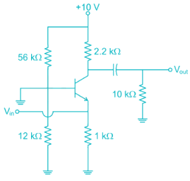
Detailed Solution for Analog Electronics - 2 - Question 6

Form DC Analysis

Since β value is large

Collector resistance = RC’ = RC ||RL

= 2.2 || 10

= 1.8 kΩ

Voltage gain = 

*Answer can only contain numeric values
Analog Electronics - 2 - Question 7


For the pnp transistor shown, the collector current IC is_______ mA.

(Assume VEB(ON) = VEB(Sat) = 0.7 V)

VEC(Sat) = 0.2 V
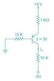

Detailed Solution for Analog Electronics - 2 - Question 7

Assume transistor is in active region

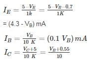
KVL in base emitter loop

0 + IB (10) + 0.7 + IE (1) = 5

IE = (1 + β)IB

IB (10 + 1 + 30) = 4.3

IC = βIB = 30 × 0.105 = 3.15 mA

VE = 5 – 1 (3.255)

= 1.745 V

VB = 1.745 – 0.7 = 1.045 V

VC = -5 + 10 (3.15) = 26.5 (not possible)

Transistor is not in active region it is  in saturation region

VEB = 0.7

VE = VB + 0.7

VEC = VB - VC = 0.2

VC = VB + 0.5


= (0.1VB + 0.55) mA

I= IB + IC

4.3 - VB = 0.1 VB + 0.1 VB + 0.55

VB = 3.13

Analog Electronics - 2 - Question 8

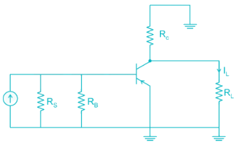
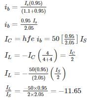
For the circuit shown in the figure if RC = 4 kΩ, RL = 4 kΩ, RB = 20 kΩ, Rs = 1 kΩ and transistor parameter are magnitude of hie = 1.1 kΩ, hfe = 50
The current gain is:
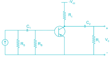
Detailed Solution for Analog Electronics - 2 - Question 8

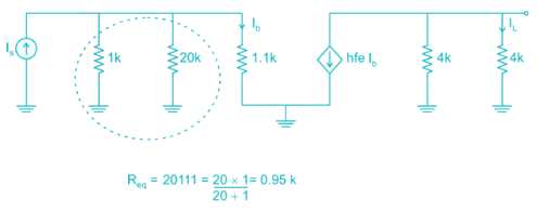
The AC equivalent circuit is:

Replacing BJT with its h-parameter model


ib using current division

iB = 0

Magnitude = |-11.65| ≈ 12

*Answer can only contain numeric values
Analog Electronics - 2 - Question 9

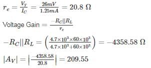
For the Common emitter configuration circuit shown below, if IC = 1.25 mA, then the magnitude of voltage gain is_______
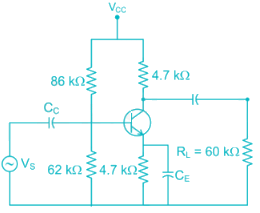

Detailed Solution for Analog Electronics - 2 - Question 9

Given RC = 4.7 kΩ, RL = 60 kΩ, Re = 4.7 kΩ, IC = 1.5 mA

Analog Electronics - 2 - Question 10

The reverse leakage current of the transistor when connected in CB Configuration is 0.3 μ A and it is 18 μA when the same transistor is connected in CE Configuration the value of α and β of the transistor for a base current of 40 mA will be respected.

Detailed Solution for Analog Electronics - 2 - Question 10


Hence α = 0.983 and β = 59

25 docs|263 tests
Information about Analog Electronics - 2 Page
In this test you can find the Exam questions for Analog Electronics - 2 solved & explained in the simplest way possible. Besides giving Questions and answers for Analog Electronics - 2, EduRev gives you an ample number of Online tests for practice

Top Courses for Electronics and Communication Engineering (ECE)

Download as PDF

Top Courses for Electronics and Communication Engineering (ECE)