Electronics and Communication Engineering (ECE) Exam > Electronics and Communication Engineering (ECE) Tests > GATE ECE (Electronics) Mock Test Series 2025 > Test: Semiconductor Diodes - Electronics and Communication Engineering (ECE) MCQ
Test: Semiconductor Diodes - Electronics and Communication Engineering (ECE) MCQ
Test Description
10 Questions MCQ Test GATE ECE (Electronics) Mock Test Series 2025 - Test: Semiconductor Diodes
Test: Semiconductor Diodes for Electronics and Communication Engineering (ECE) 2025 is part of GATE ECE (Electronics) Mock Test Series 2025 preparation. The Test: Semiconductor Diodes questions and answers have been
prepared according to the Electronics and Communication Engineering (ECE) exam syllabus.The Test: Semiconductor Diodes MCQs are made for Electronics and Communication Engineering (ECE) 2025 Exam. Find important
definitions, questions, notes, meanings, examples, exercises, MCQs and online tests for Test: Semiconductor Diodes below.
Solutions of Test: Semiconductor Diodes questions in English are available as part of our GATE ECE (Electronics) Mock Test Series 2025 for Electronics and Communication Engineering (ECE) & Test: Semiconductor Diodes solutions in
Hindi for GATE ECE (Electronics) Mock Test Series 2025 course. Download more important topics, notes, lectures and mock
test series for Electronics and Communication Engineering (ECE) Exam by signing up for free. Attempt Test: Semiconductor Diodes | 10 questions in 30 minutes | Mock test for Electronics and Communication Engineering (ECE) preparation | Free important questions MCQ to study GATE ECE (Electronics) Mock Test Series 2025 for Electronics and Communication Engineering (ECE) Exam | Download free PDF with solutions
Test: Semiconductor Diodes - Question 1

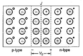
The barrier voltage (V0 or Vr) in a junction diode is the effect of
Detailed Solution for Test: Semiconductor Diodes - Question 1
Detailed Solution for Test: Semiconductor Diodes - Question 2
| 1 Crore+ students have signed up on EduRev. Have you? Download the App |
Detailed Solution for Test: Semiconductor Diodes - Question 3
Test: Semiconductor Diodes - Question 4
The most commonly used type of electron emission in electron tubes is
Detailed Solution for Test: Semiconductor Diodes - Question 5
Test: Semiconductor Diodes - Question 6
The emission of electrons in a vacuum diode is achieved by
Test: Semiconductor Diodes - Question 7
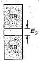
The main reason why electrons can tunnel through a p-n junction is that
Detailed Solution for Test: Semiconductor Diodes - Question 7
Detailed Solution for Test: Semiconductor Diodes - Question 8
Test: Semiconductor Diodes - Question 9
The barrier voltage for germanium is _________ at 25°C.
Detailed Solution for Test: Semiconductor Diodes - Question 9
Test: Semiconductor Diodes - Question 10
With the increase in temperature, the resistivity of an intrinsic semiconductor decreases. This is because, with the increase of temperature
Detailed Solution for Test: Semiconductor Diodes - Question 10
|
25 docs|263 tests
|
Information about Test: Semiconductor Diodes Page
In this test you can find the Exam questions for Test: Semiconductor Diodes solved & explained in the simplest way possible.
Besides giving Questions and answers for Test: Semiconductor Diodes, EduRev gives you an ample number of Online tests for practice
|
25 docs|263 tests
|
Download as PDF
Top Courses for Electronics and Communication Engineering (ECE)


Important Questions for Semiconductor Diodes
Find all the important questions for Semiconductor Diodes at EduRev.Get fully prepared for Semiconductor Diodes with EduRev's comprehensive question bank and test resources.
Our platform offers a diverse range of question papers covering various topics within the Semiconductor Diodes syllabus.
Whether you need to review specific subjects or assess your overall readiness, EduRev has you covered.
The questions are designed to challenge you and help you gain confidence in tackling the actual exam.
Maximize your chances of success by utilizing EduRev's extensive collection of Semiconductor Diodes resources.
Semiconductor Diodes MCQs with Answers
Prepare for the Semiconductor Diodes within the Electronics and Communication Engineering (ECE) exam with comprehensive MCQs and answers at EduRev.
Our platform offers a wide range of practice papers, question papers, and mock tests to familiarize you with the exam pattern and syllabus.
Access the best books, study materials, and notes curated by toppers to enhance your preparation.
Stay updated with the exam date and receive expert preparation tips and paper analysis.
Visit EduRev's official website today and access a wealth of videos and coaching resources to excel in your exam.
Online Tests for Semiconductor Diodes GATE ECE (Electronics) Mock Test Series 2025
Practice with a wide array of question papers that follow the exam pattern and syllabus.
Our platform offers a user-friendly interface, allowing you to track your progress and identify areas for improvement.
Access detailed solutions and explanations for each test to enhance your understanding of concepts.
With EduRev's Online Tests, you can build confidence, boost your performance, and ace Semiconductor Diodes with ease.
Join thousands of successful students who have benefited from our trusted online resources.
|
© EduRev
|
Education Revolution
|


|


Signup to see your scores
go up within 7 days!
Access 1000+ FREE Docs, Videos and Tests
Takes less than 10 seconds to signup