Test: Sequential Logic Circuits- 2 - Electrical Engineering (EE) MCQ
15 Questions MCQ Test GATE Electrical Engineering (EE) Mock Test Series 2025 - Test: Sequential Logic Circuits- 2

Assertion (A): The indeterminate condition of the J-K flip-flop is permitted in S-R flip-flop.
Reason (R): A J-Kfiip-flop has a characteristic similar to that of an S-R flip-flop.
Reason (R): A J-Kfiip-flop has a characteristic similar to that of an S-R flip-flop.
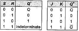
 (not indeterminate). Therefore, the indeterminate condition of the S-R flip-flop is permitted in a J-Kflip-flop.
The J-K master-slave flip-flops in figure shown below has its J and K inputs tied to + VCC and a series of pulses is applied to its CLK input.
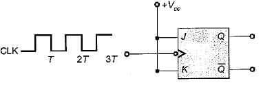
The waveform at G is given by
The waveform at G is given by
| 1 Crore+ students have signed up on EduRev. Have you? Download the App |
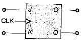
For the J-Kflip-flop shown below to function as a divide-by-2 element, the J and K inputs should be equal to
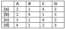
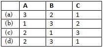
Match List-l with List-II and select the correct answer using the codes given below the lists:
List-I
A. J-K flip-flop
B. D flip-flop
C. Master-slave flip-flop
D. T flip-flop
List-lI
1. Transparent latch
2. Most versatile and widely used of all the flip flops
3. Not widely available as commercial items
4. Pulse triggered flip-flop
Codes:
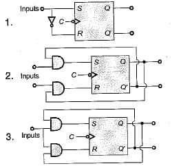
Assertion (A): An unclocked flip-flop is called a latch.
Reason (R): A latch is constructed using two cross-coupled NAND gates or NOR gates.
Consider the following statements associated with flip-flops;
1. Any one type of flip-flop can be converted to any other type by providing a suitable combinational circuit.
2. The inputs to a master-slave flip-flop must change when the clock is HIGH.
3. In a master-slave flip-flop, master is level triggered while slave is edge triggered.
4. Data lock-out flip-flops are nothing but master-slave flip-flops.
Q. Which of the statements given above is/are not correct?
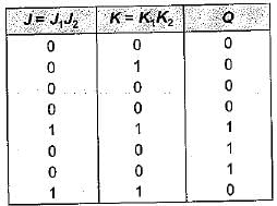
For the flip-flop shown below, there is one clock pulse for each bit time.
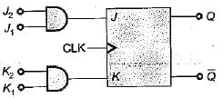
If the following serial data are applied to the flip-flop, then the resulting decimal value of the serial data that appears on the Q output will be (assume that, Q is initially ‘0’)
J1 = 01101101 ; J2 =10011011
K1 = 01101001 ; K2 = 11011011
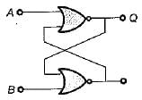
For a flip-flop formed from two NOR gates as shown in figure the unusable state corresponds to
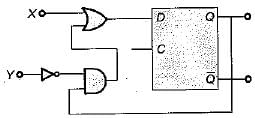
The digital circuit as shown below represents to which one of the following?

If tp is the pulse width, Δt is the propagation delay, T is period of pulse train then which of the following condition can avoid the race around condition?
Match List-I (Logic Circuit) with List-ll (Circuit Realization) and select the correct answer using the codes given below the lists:
List-I
A. J-K flip-flop
B. T flip-flop
C. D fiip-flop
List-ll
Codes:
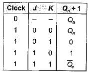
The characteristic equation of a T flip-flop is given by
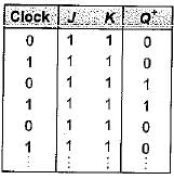
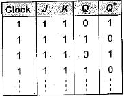
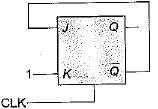
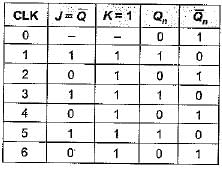
In a J-Kflip-flop we have  (shown in figure). Assuming the flip-flop was initially cleared and then clocked for 6-pulses, the sequence at the Q output will be
The output of a J-Kflip-flop Qn is ‘0’. The state of the flip-flop changes when a clock pulse is applied. The possible combination of Jn and Kn inputs could be (‘X' denote don’t care)


|
25 docs|247 tests
|
|
25 docs|247 tests
|
Top Courses for Electrical Engineering (EE)


Important Questions for Sequential Logic Circuits- 2
Sequential Logic Circuits- 2 MCQs with Answers
Online Tests for Sequential Logic Circuits- 2 GATE Electrical Engineering (EE) Mock Test Series 2025
|
© EduRev
|
Education Revolution
|


|


