Electrical Engineering (EE) Exam  >  Electrical Engineering (EE) Tests  >  Analog and Digital Electronics  >  Test: Combinational Circuits - Electrical Engineering (EE) MCQ

Test: Combinational Circuits - Electrical Engineering (EE) MCQ


Test Description

10 Questions MCQ Test Analog and Digital Electronics - Test: Combinational Circuits

Test: Combinational Circuits for Electrical Engineering (EE) 2024 is part of Analog and Digital Electronics preparation. The Test: Combinational Circuits questions and answers have been prepared according to the Electrical Engineering (EE) exam syllabus.The Test: Combinational Circuits MCQs are made for Electrical Engineering (EE) 2024 Exam. Find important definitions, questions, notes, meanings, examples, exercises, MCQs and online tests for Test: Combinational Circuits below.
Solutions of Test: Combinational Circuits questions in English are available as part of our Analog and Digital Electronics for Electrical Engineering (EE) & Test: Combinational Circuits solutions in Hindi for Analog and Digital Electronics course. Download more important topics, notes, lectures and mock test series for Electrical Engineering (EE) Exam by signing up for free. Attempt Test: Combinational Circuits | 10 questions in 30 minutes | Mock test for Electrical Engineering (EE) preparation | Free important questions MCQ to study Analog and Digital Electronics for Electrical Engineering (EE) Exam | Download free PDF with solutions
Test: Combinational Circuits - Question 1

The size of encoder required for 4 bit flash type ADC is:

Detailed Solution for Test: Combinational Circuits - Question 1

An n-bit flash type ADC requires:

1. 2n -1 comparators

2. 2n resistors

3. One 2n × n priority encoder

Here n = 4, hence the size of comparator 24 × 4

Test: Combinational Circuits - Question 2

The logic function implemented by the following 4: 1 MUX is:

Detailed Solution for Test: Combinational Circuits - Question 2

Calculation:

For the given MUX, the output is given by,

Given I0 = X, I1 = Y, I2 = X and I3 = 0

= X ⊕ Y (X-OR gate)

So, option (c)

1 Crore+ students have signed up on EduRev. Have you? Download the App
Test: Combinational Circuits - Question 3

Minimum number of Half adders, Full adders, AND gates required to implement 2 × 3 multiplier is given as

Detailed Solution for Test: Combinational Circuits - Question 3

Explanation:

Multiplier

  • A multiplier is a combinational logic circuit that we use to multiply binary digits.
  • We use a multiplier in several digital signal processing applications.
  • We use it to design calculators, mobiles, processors, and digital image processors.

Process

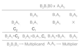
  • The first product obtained from multiplying A0 with the multiplicand is called as partial product 1.
  • And the second product obtained from multiplying A1 with the multiplicand is known as the partial product 2.

The structure of multiplication is explained below:

There are 6 product terms so to get all those 6 AND gates are required.

To get the addition of B1A0 and B0A1 we require one-half adder and this produces a carry also.

To get the addition of B2A0, B1A1 and C1 we require Full adder because of 3 inputs and this also produces a carry.

To get the B2A1 and C2 we require one-half adder because of 2 inputs.

Conclusion:


Total 6 AND gates2 Half adders and 1 Full adder are required.

Test: Combinational Circuits - Question 4

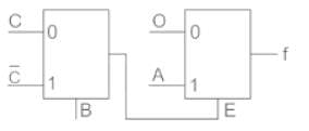
The Boolean function ‘f’ implemented as shown in the figure using two input multiplexers is:
Detailed Solution for Test: Combinational Circuits - Question 4

Concept:

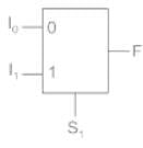
For a 2 × 1 MUX is shown above, the output function F is expressed as:

i.e. when S1 = 0, I0 is transmitted to the output.

And when S1 = 1, I1 is transmitted to the output.

Application:

The output of the 1st MUX will be:

The final output will be:

Test: Combinational Circuits - Question 5

Construct a 16 × 1 multiplexer using 2 × 1 multiplexer. How many 2 × 1 multiplexer are required to construct?

Detailed Solution for Test: Combinational Circuits - Question 5

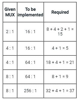
To implement 2n × 1 MUX using 2 × 1 MUX, the total number of 2 × 1 MUX required is (2n - 1).

∴ The number of 2 × 1 multiplexer required to implement 16 × 1 MUX will be:

n = 16 - 1 = 15

Or we can follow the below steps to calculate the same:

1st stage = 16/2 = 8

2nd  stage = 8/2 = 4

3rd stage = 4/2 = 2

4th stage = 2/2 = 1

The sum will give the total number of MUX required to implement 16 × 1 multiplexer using 2 × 1, i.e.

n = 8 + 4 + 2 + 1 = 15
Important Point

Test: Combinational Circuits - Question 6

Consider the multiplexer based logic circuit shown in the figure.
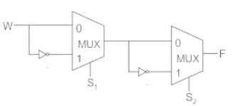
Which one of the following Boolean functions is realized by the circuit?

Detailed Solution for Test: Combinational Circuits - Question 6

Concept:

For a 2 × 1 MUX is shown above, the output function F is expressed as:

i.e. when S1 = 0, I0 is transmitted to the output.

And when S1 = 1, I1 is transmitted to the output.

Application:
The given circuit is redrawn as:


Now, the required function f will be:

Test: Combinational Circuits - Question 7

Which device converts, a decimal input number to binary

Detailed Solution for Test: Combinational Circuits - Question 7

An encoder converts information from one format or code to another. An encoder can be used to encode the decimal number to binary number.

Additional Information

Accumulator:

  • An accumulator is a general-purpose register of microprocessor. It is used to store result of most arithmetic and Logical Operations performed in 8085.

Some examples of decimal to binary conversion are:

  • 0 → 0
  • 1 → 01
  • 2 → 10
  • 3 → 11
  • 4 → 100
  • 5 → 101
  • 6 → 110
  • 7 → 111
  • 8 → 1000
  • 9 → 1001

ALU:

  • ALU stands for arithmetic logic unit. ALU contains circuits that perform arithmetic operations such as Addition/subtraction and Logical operations such as XOR, AND etc

Memory:

  • Memory is a storage device that is used to store data as well as instructions that are to be executed by the microprocessor.
Test: Combinational Circuits - Question 8

The output 'Y' of the combinational circuit shown below is
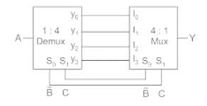
Detailed Solution for Test: Combinational Circuits - Question 8


Y = 1

Test: Combinational Circuits - Question 9


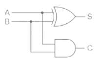
For the circuit shown, find the expression for 's'?

Detailed Solution for Test: Combinational Circuits - Question 9

Concept:

From the given figure:


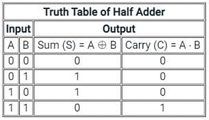
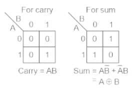
The above circuit is of Half adder:

  • Sum (S) can be obtained by: A XOR B = A⨁ B
  • Carry (C) can be obtained by: A AND B = A ∙ B​​​​​​


From the above truth table, it can conclude that:


Fig: K-Map simplification of Half Adder

Test: Combinational Circuits - Question 10


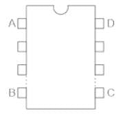
In the above image of IC (integrated chip) identify the pin number 1?

Detailed Solution for Test: Combinational Circuits - Question 10

Normally we see a half circle mark on IC's one edge. That edge is the top of the IC.

And if we keep IC in the below manner,


Then the first left side pin is Pin no. 1

Here, pin no. 1 is A

Additional Information

  • Integrated Circuits are made up of Silicon.
  • Integrated circuits are the chips of Silicon on which transistors,
    logical gates, resistors or capacitors are embedded.
  • First IC was developed by Jack Kilby and Robert Noyce in 1958,
    but the concept was introduced by Geoffrey Dummer in 1952.
  • These building blocks of a circuit can act as microprocessors, amplifiers, memory etc.
137 videos|143 docs|71 tests
Information about Test: Combinational Circuits Page
In this test you can find the Exam questions for Test: Combinational Circuits solved & explained in the simplest way possible. Besides giving Questions and answers for Test: Combinational Circuits, EduRev gives you an ample number of Online tests for practice

Top Courses for Electrical Engineering (EE)

137 videos|143 docs|71 tests
Download as PDF

Top Courses for Electrical Engineering (EE)