Basics of MOSFET | Electronic Devices - Electronics and Communication Engineering (ECE) PDF Download
MOSFET
Metal Oxide Silicon Field Effect Transistors commonly known as MOSFETs are electronic devices used to switch or amplify voltages in circuits. It is a voltage controlled device and is constructed by three terminals. The terminals of MOSFET are named as follows:
- Source
- Gate
- Drain
- Body

MOSFET Construction
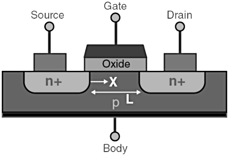
The circuit of MOSFET is typically represented as follows:

- The p-type semiconductor forms the base of the MOSFET.
- The two types of the base are highly doped with an n-type impurity which is marked as n+ in the diagram.
- From the heavily doped regions of the base, the terminals source and drain originate.
- The layer of the substrate is coated with a layer of silicon dioxide for insulation.
- A thin insulated metallic plate is kept on top of the silicon dioxide and it acts as a capacitor.
- The gate terminal is brought out from the thin metallic plate.
- A DC circuit is then formed by connecting a voltage source between these two n-type regions.
Working Principle of MOSFET
When voltage is applied to the gate, an electrical field is generated that changes the width of the channel region, where the electrons flow. The wider the channel region, the better conductivity of a device will be.
MOSFET Types
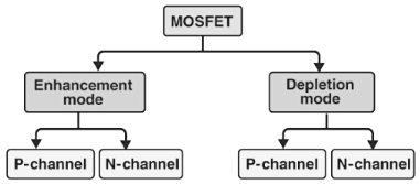
The classification of MOSFET based on the construction and the material used is given below in the flowchart.

MOSFETs are of two classes: Enhancement mode and depletion mode. Each class is available as n-channel or p-channel; hence overall they tally up to four types of MOSFETs.
Depletion Mode
When there is no voltage across the gate terminal, the channel shows maximum conductance. When the voltage across the gate terminal is either positive or negative, then the channel conductivity decreases.
Enhancement Mode
When there is no voltage across the gate terminal, then the device does not conduct. When there is the maximum voltage across the gate terminal, then the device shows enhanced conductivity.
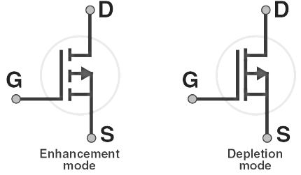
The N-channel MOSFETs are abbreviated as NMOS and are symbolically represented as shown in the figure below:

Similarly, the P-channel MOSFETs are abbreviated as PMOS and are symbolically represented as follows:
Operating Regions of MOSFET
A MOSFET is seen to exhibit three operating regions. Here, we will discuss those regions.
Cut-Off Region
The cut-off region is a region in which there will be no conduction and as a result, the MOSFET will be OFF. In this condition, MOSFET behaves like an open switch.
Ohmic Region
The ohmic region is a region where the current (IDS)increases with an increase in the value of VDS. When MOSFETs are made to operate in this region, they are used as amplifiers.
Saturation Region
In the saturation region, the MOSFETs have their IDS constant in spite of an increase in VDS and occurs once VDS exceeds the value of pinch-off voltage VP. Under this condition, the device will act like a closed switch through which a saturated value of IDS flows. As a result, this operating region is chosen whenever MOSFETs are required to perform switching operations.
MOSFET as a Switch
MOSFETs are commonly used as switches. The circuit below shows the configuration of MOSFET when it is used as a switch.

In the circuit arrangement, an Enhancement-mode N-channel MOSFET is used to switch a simple lamp “ON” and “OFF.” The input fate voltage Vgs is adjusted to an appropriate positive voltage to switch “ON” the device and the voltage level is set to a negative value or zero to turn it “OFF.”
The switching characteristics for both N-channel and P-channel type MOSFET are summarised in the table below:
MOSFET vs BJT
In this section, let us discuss some differences between MOSFET and BJT.
MOSFET applications
- Radiofrequency applications use MOSFET amplifiers extensively.
- MOSFET behaves as a passive circuit element.
- Power MOSFETs can be used to regulate DC motors.
- MOSFETs are used in the design of the chopper circuit.
Advantages of MOSFET
- MOSFETs operate at greater efficiency at lower voltages.
- Absence of gate current results in high input impedance producing high switching speed.
Disadvantages of MOSFET
- MOSFETs are vulnerable to damage by electrostatic charges due to the thin oxide layer.
- Overload voltages make MOSFETs unstable.
|
21 docs|29 tests
|
FAQs on Basics of MOSFET - Electronic Devices - Electronics and Communication Engineering (ECE)
| 1. What is a MOSFET and how does it work? |  |
| 2. What are the advantages of using MOSFETs in electronic circuits? |  |
| 3. How do you calculate the drain current of a MOSFET? |  |
| 4. What is the significance of the threshold voltage in a MOSFET? |  |
| 5. How does the MOSFET operate in different regions: cutoff, triode, and saturation? |  |

|
Explore Courses for Electronics and Communication Engineering (ECE) exam
|

|


