Carrier Transport GATE PYQs | Electronic Devices - Electronics and Communication Engineering (ECE) PDF Download
Q.1. An abrupt pn junction (located at x = 0) is uniformly doped on both p and n sides. The width of the depletion region is W and the electric field variation in the x-direction is E(x). Which of the following figures represents the electric field profile near the pn junction?
(a) 
(b) 
(c) 
(d) 
Correct Answer is Option (a)
- IF Left side is p-region and right side is n-region then electric field triangle will be down warded
- If Left side is n-region and right side is p-region, then electric field triangle will be upward.
Q.2. Consider a silicon sample at T = 300K, with a uniform donor density Nd = 5 x 1016 cm-3 illuminated uniformly such that the optical generation rate is Gopt = 1.5 x 1020 cm-3 s-1 throughout the sample. The incident radiation is turned off at t = 0. Assume low-level injection to be valid and ignore surface effects. The carrier lifetimes are тpo = 0.1 μs and Tno = 0.5 μS
(a) 1.5 x 1013 cm-3 and 7.47 x 1011 cm-3
(b) 1.5 x 1013 cm-3 and 8.23 x 1011 cm-3
(c) 1.5 x 1013 cm-3 and 3.73 x 1011 cm-3
(d) 7.5 x 1013 cm-3 and 4.12 x 1011 cm-3
Correct Answer is Option (a)
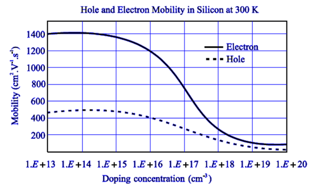
Q.3. A piece of silicon is doped uniformly with phosphorous with a doping concentration 1016 /cm3. The expected value of mobility versus doping concentration for silicon assuming full dopant ionization is shown below. The charge of an electron is 1.6 x 10⁻¹⁹ C.
The conductivity (in S cm–1) of the silicon sample at 300 K is____
Hole and Electron Mobility in Silicon at 300 K
 (a) 1.82
(b) 1.92
(c) 192
(d) 150.2
Correct Answer is Option (b)
Q.4. Consider a region of silicon device of electrons and holes, with an ionized donor density of Nd+ = 1017 cm-3. The electric field at x = 0 is 0 V/cm and the electric field at x = L is 50 kV/cm in the positive x direction. Assume that the electric field is zero in the y and z directions at all points.
Given q = 1.6 x10⁻¹⁹ coulomb,
∈0 = 8.85 x 10⁻¹⁴ F/cm,
∈r = 11.7
for silicon, the value of L in nm is_____
Ans. 32.372 x 10⁻⁹ m
Q.5. A dc voltage of 10 V is applied across an n-type silicon bar having a rectangular cross-section and a length of 1 cm as shown in figure. The donor doping concentration ND and the mobility of electrons μn are 1016 cm-3 and 1000 cm2V–1s–1, respectively. The average time (in μs) taken by the electrons to move from one end of the bar to other end is__________ (a) 100
(b) 200
(c) 300
(d) 400
Correct Answer is Option (a)
Given,
= 104 cm/s
Q.6. Electric Field of 1 V/m is applied to a Boron doped Silicon semiconductor slab having doping density of 1016 atoms/cm3 at 300K temperature. Determine the approcimate resistivity of the slab. (Consider intrinsic carrier concentration of Silicon at 300 K = 1.5 x 10¹⁰ / cm3 Hole Mobility = 500 cm2/Vs at 300 K; Electron Mobilty = 1300 cm2/Vs at 300 K).
(a) 0.48 Ω-cm
(b) 0.35 Ω-cm
(c) 0.16 Ω-cm
(d) 1.25 Ω-cm
Correct Answer is Option (d)
Conductivity of extrinsic semiconductor (σ)= nqμn + pqμp
here , n and p are no. of electrons and protons respectively
q = 1.6 x 10⁻⁹ C
μn = 1300 cm2/Vs
μp = 500 cm2/Vs
As it is Boron doped Silicon semiconductor so it is p-type.
Therefore p = NA = 1016 atoms/cm3
Using mass action law , n = ni2/NA
Then , σ = 1.6 x 10⁻⁹ (nμn + pμp)
, 8 x 10⁻¹
Resistivity (ρ) = 1/σ
= 1.25 Ω-cm
|
21 docs|29 tests
|

|
Explore Courses for Electronics and Communication Engineering (ECE) exam
|

|


