Chapter 8 - Power Electronics (Part - 1) - Mechanical Engineering PDF Download
1. Basics of Power Semiconductor Devices
Basic Power Electronic Circuit Block Diagram
The output of the power electronic circuit may be variable dc/variable ac voltage/ variable frequency. The feedback component measures parameters of load like speed in case of a rotating machine. Block diagram of a typical power electronic system
Power Semi-Conductor Devices
Power semi-conductor devices should ideally constitute following characteristics
Must be able to carry large current
- ON resistance should be lower (ideally 0) to reduce heat dissipation
- OFF resistance should be higher (ideally ∞) to withstand switching transients
- They must carry large currents with uniform distribution of current over device's area to avoid localized heating and breakdown
- Device should be capable of high switching speed.
- Faulty switching due to applied voltage transient should not happen
Based on their operating characteristics, power semiconductor devices can be classified as below
- Uncontrolled Devices
- Controlled Devices
- Semi-Controlled Devices
Power Diodes
Power diodes belong to the class of uncontrolled power semiconductor devices. They are similar to low power p-n junction diodes called signal diodes. However to make them suitable for high power applications they are constructed with n- layer between p+ and n+ layers to support large blocking voltage by controlling the width of depletion region. They can be used as freewheeling diodes in ac to dc conversion. Peak inverse voltage is defined as largest reverse voltage that a diode can be subjected to.
Power diodes can also be classified as below based on their use case
- General Purpose Diodes
- Fast Recovery Diodes
- Schottky Diodes
Reverse Recoveiy Characteristics
 Reverse recovery characteristics of a power diode
Reverse Recovery
Time When a diode is changed from forward biased state to reverse biased state, the diode continues to conduct in the reverse direction because of stored charges in two layers. The reverse current flows for reverse recovery time, trr.
Reverse recovery time, trr = ta + tb
Where ta is time for diode current to reach IRM from 0,
tb is the time for diode current to reach 1/4 IRM from lRM.
In time ta, charge in depletion region is removed, hence the current through diode decays thereafter. During tb, charge from two semiconductor layers is removed
Softness Factor
Softness factor is a measure of voltage transients that occur during the time diode recovers.
S = tb/ta
Table. Classification of diode based on softness factor
Charge Stored in Depletion Region
Let QR be the charge stored in depletion region of power diode.


Power Transistors
Power transistor is a current controlled device and the control current is made to flow through base terminal. Thus the device can be switched ON or OFF by applying a positive/negative signal at base. Switching characteristics of a power transistor
Different quantities related to switching characteristics of a power transistor are given below.
- Delay time, td - time taken for the collector saturation current, lCS to start rising
- Rise time, tr - time taken for the collector current to reach lCS
- Storage time, ts - time taken for charges to be removed from depletion region
- Fall time, tf - time taken for collector current to fall to 0
- ON time, tON = td + tr
- OFF time, tOFF = ts + tf
Power MOSFET
MOSFET is a voltage controlled device. As its operation is based on flow of majority carriers only, MOSFET is a unipolar device. As power MOSFET is unipolar device, there is no minority storage effect so that high switching speed is possible. Here switching speed is limited by inherent capacitance only. Also due to large drain area, secondary breakdown and thermal runaway that destroy the device do not occur. Switching characteristics of MOSFET
Table. Comparison of features of BJT & MOSFET
IGBT
IGBT refers to insulated gate bipolar transistor. It combines advantages of both MOSFET and BJT. So IGBT has high input impedance (similar to MOSFET) and lower on-state power loss (similar to BJT). Also IGBT is free from secondary breakdown problem present in BJT
Silicon Controlled Rectifier (SCR)
It is a four layer three junction p-n-p-n device and has three terminals; anode, cathode and gate. SCR can be turned on by using a gate signal controlling the charge near the p-n junctions. Hence SCR is a charge controlled device. However, SCR cann't be turned off by using gate signal. Thus SCR belongs to the class of semi-controlled semi-conductor device. Schematic diagram and circuit symbol of SCR
Operating Modes
Reverse Blocking Mode In this mode, terminal K is positive with respect to terminal A and also the gate terminal is open. Hence the junctions, ]1 and J3 are reverse biased and \2 is forward biased.
Forward Blocking
Mode In this mode, terminal A is positive with respect to terminal K and gate terminal is open. Hence junctions J1 and J3 are forward biased and J2 is reverse biased in this mode.
Forward Conduction Mode
A thyristor is brought from forward blocking mode to forward conduction mode by increasing VAK above VBO or by applying a gate pulse between gate and cathode. In this mode, thyristor is in on-state and behaves like a closed-switch. Static V-I characteristics of SCR
Thyristor Turn-On Methods
All the thyristor methods involve increasing carriers near junction J2. When anode is positive with respect to cathode, thyristor can be turned on by any of the methods listed below;
- Forward Voltage Triggering
- Gate Triggering
- dv/dt Triggering
- Temperature Triggering
- Light triggering
Switching Characteristics of Thyristor

 Switching characteristics of thyristor
Two Transistor Model of a Thyristor
The thyristor operating principle can be explained using two-transistor analogy. The two transistor model is obtained by bisecting two middle layers, along the dotted line into two separate halves.
 Two transistor model of thyristor
Let ICBOi. , ∝i correspond to leakage current and collector base current gain of transistor Qj.
Thyristor Protection
di/dt Protection
During turn-on, when anode current spreads across whole of junction. If di/dt is higher than spread of carriers, local hot spots may appear damaging the device. Above can be avoided by using an inductor in series with SCR.
dV/dt Protection
During the forward blocking state, junctions J1 and J3 of SCR are forward biased and junction J2 is reverse biased. In this mode, junction J2 acts as a capacitor.
lf dVa/dt is high, SCR may get turned on. To prevent this false trigger, snubber circuit is connected in parallel with thyristor Demonstration of dv/dt protection.
Series / Parallel Connection of Thyristor
When a number of thyristors are connected in series or parallel, the overall utilization of SCRs can be expressed using below, where n is the number of SCRs in string.
Derating factor, DRF = 1 - string efficiency.
Firing Circuits for Thyristor
Using Pulse Transformer
Figure below gives brief idea of thyristor triggering circuit using pulse transformer. Pulse generator is used to generate control signal for triggering of thyristors. The control signal generated by pulse generator may not be able to turn on SCR. Hence pulse amplifier is used for reliable triggering of SCRs. Pulse transformer is helpful to isolate low voltage gate cathode circuit from high voltage anode cathode circuit. Firing circuit using pulse transformer
Resistance Firing Circuit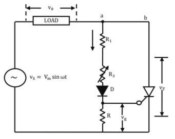
 Resistance firing circuit
Let VgP be the peak value of gate voltage and Vgt be the trigger voltage for thyristor.

Also for the SCR to be triggered, following condition should be satisfied, Vgp > Vgt
Hence SCR can be just triggered for ∝ = 90° if Vgp = Vgt.
RC Firing Circuit (Half Wave)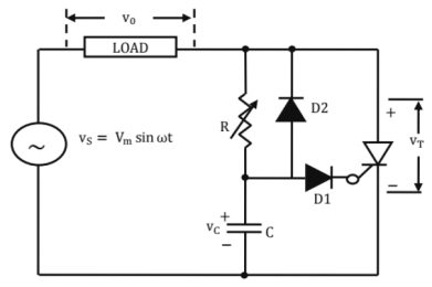
 RC half wave triggering circuit and corresponding waveforms
RC Firing Circuit (Full Wave)
In this case, input supply is rectified using bridge rectifier before being applied to gate terminal of SCR. So VC(t) takes a minimum value of zero, but not -Vm as in case of half wave RC firing circuit. Also the SCR is triggered in every half cycle due to the rectified input.
UJT Oscillator Triggering
For 0 < t < T1, capacitor charges through R from Vv to VP with a time constant RC. During this charging, emitter circuit of UJT acts as open circuit. At T1, E - B1 breaks down and capacitor discharges through R1 with a time constant R1C.

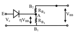
 UJT oscillator trigger circuit
Gate Pulse Amplifiers
Gate pulse amplifiers use pulse transformer for isolating gate circuit from anode circuit. But these are not suitable for RL load because the triggering point is not known exactly. Circuit diagram of a gate pulse amplifier
Pulse Train Gating
As gate pulse amplifiers cannJt be used for R-L loads due to high losses, pulse train gating is used. Because of train of pulses, thyristor losses are reduced. Circuit diagrams and waveforms corresponding to pulse train gating
Thyristor Commutation
Commutation is defined as process of turning off a thyristor. Thyristor commutation is a necessary mechanism for obtaining the controlled output in many of the thyristor circuits. As thyristor is a semi-controlled device, it can not be turned off directly by gate signal. Hence external means are required for turning off thyristor. As discussed, thyristor turn-off requires that anode current falls below holding current and a reverse voltage is applied to thyristor for sufficient time to enable it to recover to blocking state.
Thyristor Commutation Techniques
Class- A /Load Commutation
Here the elements L & C are chosen such that, circuit is underdamped. Hence, the current through the load decays to zero in finite-time and thyristor gets turned-off. For low values of RH elements L and C are connected in series for commutation. For high values of R, capacitor element is connected in parallel with R for commutation.
 Class A or load commutation (a) series capacitor (b) shunt capacitor.
Class-B /Resonant Pulse Commutation Resonant-pulse commutation (a) circuit diagram (b) waveforms

Vab = Vs cos (ω0(t3 - t2))
circuit turn-off time for thyristor,
Class-C/Complementaiy Commutation
 Class-C commutation


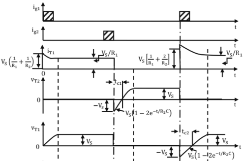
 Waveforms corresponding to dass-C commutation
Class-D/Impulse Commutation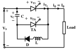
 Gass D commutation (a) Circuit diagram (b) waveforms
Circuit turn -off time for
Class-E/External Pulse Commutation
In this type of commutation, a pulse of current from a separate voltage source is used to turn-off SCR. Here the peak value of current must be more than load current for commutation. External-pulse commutation circuit
For reliable operation, Vs = 2V1 < 0 ⇒ Vs < 2V1
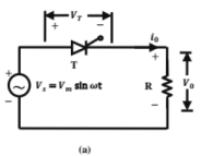
Class - F/ Line Commutation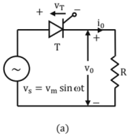
 Class F commutation (a) circuit diagram (b) waveforms
2. Phase Controlled Rectifier
Introduction
Firing angle is the angle between the instant that thyristor would conduct if it were a diode and the instant at which it's triggered. It's denoted by ∝. In phase controlled rectifiers, firing angle is varied to get the controllable dc power. The period for which thyristor is reverse biased in thyristor circuits is known as turn-off time. ltJs denoted by tc. It's mainly the time for which voltage across the thyristor is negative.
Table, classification of converters
 (a) One-quadrant converter and (b) two-quadrant converter
Single phase half wave controlled rectifier with R load
 Single-phase half-wave thyristor circuit with R load (a) circuit diagram and (b) voltage and current wave forms.


- tc = π/ω sec

Single Phase Half Wave Converter with R-L Load
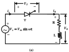
 Single-phase half-wave circuit with RL load and a freewheeling diode, (a) circuit diagram and (b) voltage and current waveforms.
Single Phase Half Wave Converter with R-L Load And Free wheeling Diode
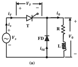
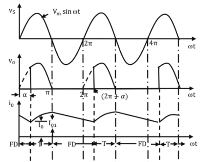
 Single-phase half-wave circuit with RL load and a freewheeling diode, (a) circuit diagram and (b)voltage and current waveforms.


- turn-off time, tc = π/ω
Following are the advantages of using freew heeling diode in parallel with R - L load.
- Input pf is improved
- Load current waveform is improved
- Load performance is better.
Single Phase Half Wave Converter with RLE Load
The minimum value of firing angle at which T can be triggered can be given as,
If SCR is triggered for firing angle ∝ < θ1, it will not be turned on as it's reverse biased. Similarly the maximum value of firing angle is, θ2 = π - θ1.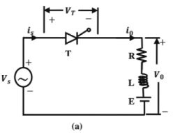
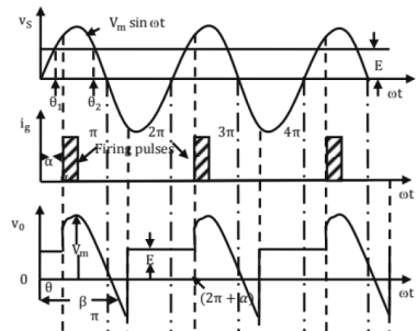
 Single-phase half-wave circuit wit RLE load (a) circuit diagram and (b) voltage and current waveforms.
- Idc = 1/2πR [Vm(cos α - cos(γ + a)) - E.γ]
- Vodc = 1/2π [Vm(cos α - cosβ) + E(2π + a - β)]

- tc = (2π - β)/ω
In single phase rectifiers, if supply has a frequency f output voltage has a ripple frequency of f.
Single Phase Full-Wave Mid-Point Converter
Single phase full wave mid - point converter falls in the class of single - phase two pulse converter.
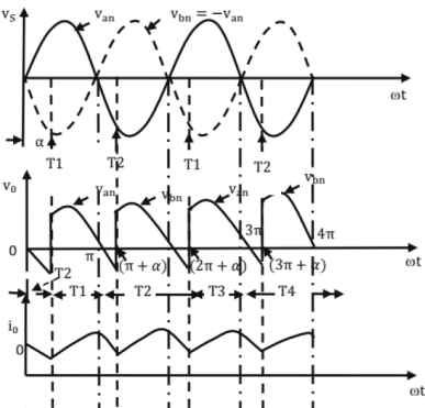
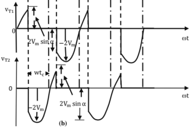


- PIV = 2Vm
Single Phase Full-Wave Bridge Converter with RLE Load
Single-phase full wave bridge converter falls into class of 2-phase converter. But it requires 4 SCRS, with relatively lesser P1V rating as compared to mid-point converter.
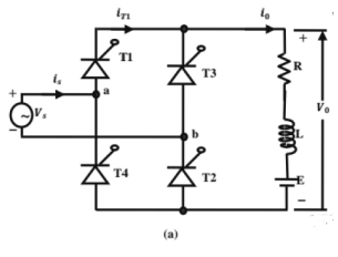

 Single-phase full converter bridge with RLE load (b) voltage and current waveforms for continuous load current


- PIV = 2Vm
Single Phase Semi-Converter with R-L-E Load

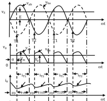
 Single-phase semiconverter bridge (a) power-circuit diagram with RLE load and (b) voltage and current waveforms for continuous load current.
- Vodc = Vm/π (1 + cos α)
- tc = (π - α)/ω
 Converter output voltage as a function of firing of angle for semi and full converters.
Three Phase Half-Wave Converter
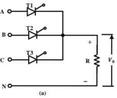
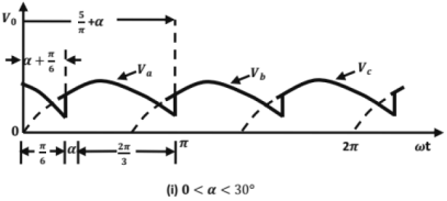
 (a) 3-phase half-wave SCR converter and (b) its output voltage waveforms for (i) 0 < α < 30° and (ii) 30 < α < 150°

Three Phase Full Converter
 Power circuit for a 3-phase full-converter feeding RLE load.

 Voltage and current waveforms for a 3-phase full-converter for ∝ = 60s.

Average value of source current,
Average value of thyristor current,
Dual Converters
Dual converters are those whose average values of output voltage and output currents can be positive as well as negative.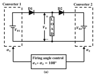
 (a) Equivalent circuit of an ideal dual converter (b) Variation of terminal voltage for an ideal dual converter with firing angle.
3. Choppers
Introduction
A.C. link chopper constitutes a inverter to convert fixed dc voltage to variable ac voltage and a phase controlled rectifier to get variable dc output. A dc chopper converts fixed dc voltage to variable dc voltage directly, through one stage conversion.
Principle of Operation
A chopper is a high speed on / off semiconductor switch. It connects source to load and disconnects load from source at faster speed. The inductor is used in series with load for minimum load current variation. Also a freewheeling diode, FD is connected in anti-parallel fashion with the load to freewheel the load current when SW is off.
 Elementary chopper circuit
 Output voltage and current waveforms.
Average load voltage,

where a = TON/T is duty cycle, T - TON + Toff is chopping period and f = 1/T is chopping frequency.
Variation of Load Current
For low values of L
When inductance, L is smaller, i0(t) varies in exponential manner
Per unit - ripple current
R, is load resistance and L is the inductance in serise with R. Per unit ripple current as a function of a and T/Ta
For High Values of L
If inductance, L is large, i0(t) varies in linear manner due to larger time constant of load.
Control Strategies
Constant Frequency System
In this scheme, TON is varied, keeping T constant. This is also called pulse- width modulation (PWM)/Time ratio control (TRC).
Variable Frequency System
In this scheme, chopping frequency, f is varied by keeping TON or TOFF constant. This method controlling ∝ is also called as frequency modulation scheme.
FM scheme has following disadvantages as compared to PWM scheme.
- f has to be varied over wide range for controlling V0 in frequency modulation. Filter design for such a wide variation is difficult.
- Larger Toff may lead to discontinuous load current.
- For control of ∝, frequency variation should be wide. So there is a possibility of interference with signaling and telephone lines in frequency modulation scheme.
Step - Up Chopper (or Boost Converter)
 Step-up chopper circuit

Thyristor Chopper Circuits
Thyristor chopper circuits can also be classified based on commutation mechanisms. In DC choppers, it is essential to provide a separate commutation circuitry to commutate the main power SCR.
- Forced commutation
(a) Voltage commutation
(b) Current commutation - Load commutation


