Circuits Analysis & Applications of Diodes, BJT, FET & MOSFET - 1 | Analog Circuits - Electronics and Communication Engineering (ECE) PDF Download
| Table of contents |
|
| Diode |
|
| Applications of Diodes |
|
| Junction Transistor |
|
| Current Relationship in BJT |
|

Diode
- An ideal diode may be considered as a most fundamental nonlinear element.
- An ideal diode is simply a PN junction where the change from p-type to the n-type material is assumed to occur instantaneously. Ideal Diode:
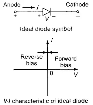
- Silicon and germanium diodes exhibit a cut-in voltage of 0.6 V and 0.2 V respectively in their characteristic curves and thus approximate closely the ideal diode in this respect.
- The Peak Inverse Voltage (PIV) is the highest reverse voltage that diode can withstand before breaking down and permitting current to flow in the reverse direction.
➤ Semiconductor Diode:
- The two types of semiconductor materials n-type and p-type are chemically combined to form a p-n junction.
- A region near the junction is without any free charge particles called depletion.
➤ Biasing of a Diode:
- The electric field across the junction has a constant polarity called barrier potential.
- A popular semiconductor device is formed using a p-n junction called p-n junction diode.
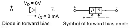
- No Applied Bias (VD = 0 V ): In absence of applied bias voltage, the net flow of charge in any direction for a semiconductor diode is zero.
- Forward Bias (VD > 0V ): In forward biased condition, when applied voltage approaches barrier potential, the depletion region reduces as forward bias increases.
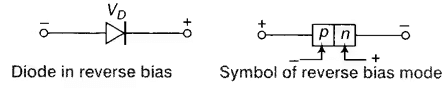
- Reverse Bias: While in reverse biased condition, the depletion region widens and minority carriers carry the current called reverse saturation current denoted as I0.
- The breakdown in Diode: If reverse biased voltage increases, at a particular voltage breakdown occurs due to accelerated minority charge particles. This is called avalanche effect. For a heavily doped diode, the electric field across the depletion region is extremely intense to pull the electrons out of valence bands. This effect is known as Zener effect.
Circuit Analysis of Diodes
There are three different techniques that are used to analyse circuits that contain diodes:
- Load line analysis should be used only when you have an I-V characteristic for the diode
- Piece-wise models are used to estimate the diode current and voltage
- The accuracy of this, depends on the region of operation and the use of the series resistors, Rs and Rz
Applications of Diodes
- Radio demodulation: an AM signal consists of alternating positive and negative peaks of voltage, whose amplitude or “envelope” is proportional to the original audio signal, but whose average value is zero. The diode rectifies the AM signal, leaving a signal whose average amplitude is the desired audio signal.
- Power conversion: This type of rectifiers are constructed from diodes, where they are used to convert alternating current (AC) electricity into direct current (DC). Automotive alternators are an example, where the diode provides better performance than the commutator of the earlier dynamo.
- Over-voltage protection: Many integrated circuits also incorporate diodes on the connection pins to prevent external voltages from damaging their sensitive transistors. Specialised diodes are operate to protect from over-voltages at higher power.
- Ionising radiation detectors, Temperature measuring, Current steering etc.
Junction Transistor
- Both the electrons and holes take part in the conduction process for bipolar devices.
- BJT consists of two p-n junctions manufactured in a special way and connected in series, back to back.
- The transistor is generally a 3-terminal device with emitter, base and collector terminals.
- From the physical structure, BJTs can be divided into 2 groups: NPN and PNP transistors.
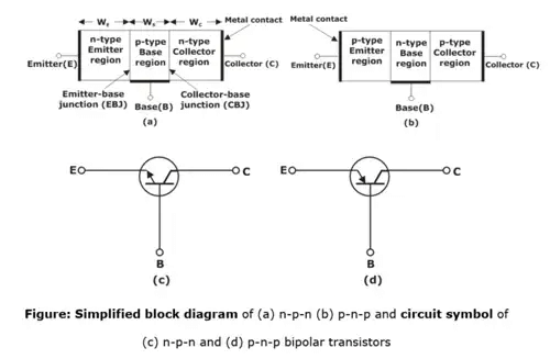
- Modes of operation: The transistor consists of two p-n junctions, the emitter-base junction (EBJ) and the collector-base junction (CBJ). Depending on the bias condition (forward or reverse) of each of these junctions, different modes of operation of BJT are obtained, as shown in below table.
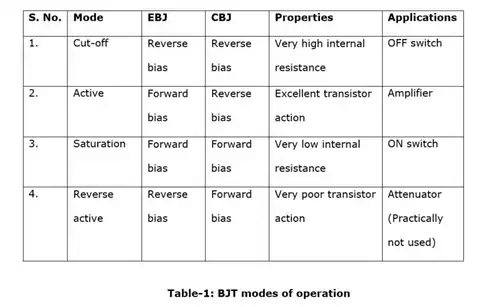
- Active Mode:
When the emitter-base junction of the transistor is forward biased and the collector-base junction is reverse biased, the transistor operates in active region.In this mode transistor is used as amplifier. This bias configuration is shown in below figure for n-p-n and p-n-p transistors.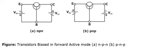
- Saturation Region
When both the emitter-base junction and collector-base junction are forward biased, the transistor operates in saturation region. Transistor has a large current in saturation mode. In the saturation mode , the trasnsitor is used as closed switch.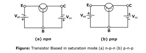
- Cut-off region
When both the emitter-base and collector-base junctions are reverse biased, transistor operates in cut-off region. In cut-off mode the current through the transistor is zero(ideally). In this case the transistor is operated as an open switch. Both n-p-n and p-n-p transistor are biased in cut-off mode as shown in below figure.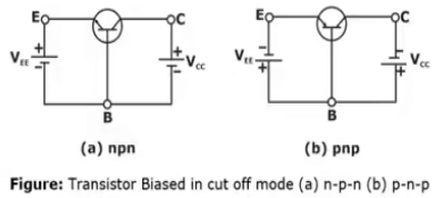
- Reverse Active Region or Inverse Region
When the emitter-base junction of the transistor is reverse biased and the collector-base junction is forward biased, the transistor is said to be in reverse active mode. This mode of operation is not often used. In below figure, transistors are biased in reverse active mode.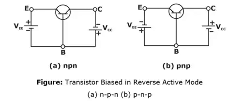
Current Relationship in BJT
If Bipolar transistor is treated as single node, they by Kirchhoff's current law
IE = IC + IB
This relation is applicable in all three configurations of BJT.
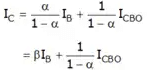
➤ Relation between current gain
For dc mode, common emitter current gain
β = IC/IB
And common base current gain
α = IC/IE
Applying these expressions in above equation,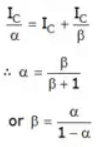
➤ Relation between leakage current
For common emitter configuration,
IC = α(IC+IB) + ICBO
⇒ IC = α(IC + IB) + ICBO (IE = IC = IB)
⇒ (1 - α)IC = αIB + ICBO
⇒ 
Since the current equation for the common base configuration is as
IC = βIB + ICEO
Comparing above both equations,
ICEO = ICBO/1-α
or ICEO = (1 + β)ICBO
Example: A transistor has IB = 25 μA, β = 100, ICBO = 100 nA. Calculate a, IC, IE and ICEO.
Solution: β = 100
α = β/(1+β) = 100/101 = 0.99
IC = βIB + (1+β)ICO
= 100 x 25 x 10-6 + 101 x 10-9 = 2.51 mA
IE = -(IB + IC)
IE = -(0.025 + 2.51) = -2.535 mA
ICEO = ICBO + (1+β) = 101 x 100 x 10-9 = 10.1μA
|
3 videos|75 docs|64 tests
|
FAQs on Circuits Analysis & Applications of Diodes, BJT, FET & MOSFET - 1 - Analog Circuits - Electronics and Communication Engineering (ECE)
| 1. What is the application of diodes? |  |
| 2. How does a diode work? | |
| 3. What is the purpose of a junction transistor? | |
| 4. What is the current relationship in a BJT circuit? | |
| 5. What are the applications of BJT? | |


study material
,shortcuts and tricks
,Circuits Analysis & Applications of Diodes
,MCQs
,Objective type Questions
,Free
,Semester Notes
,Sample Paper
,mock tests for examination
,FET & MOSFET - 1 | Analog Circuits - Electronics and Communication Engineering (ECE)
,Summary
,practice quizzes
,past year papers
,Extra Questions
,Viva Questions
,Circuits Analysis & Applications of Diodes
,FET & MOSFET - 1 | Analog Circuits - Electronics and Communication Engineering (ECE)
,BJT
,ppt
,BJT
,FET & MOSFET - 1 | Analog Circuits - Electronics and Communication Engineering (ECE)
,BJT
,Exam
,video lectures
,Circuits Analysis & Applications of Diodes
,Important questions
,Previous Year Questions with Solutions
;


Circuits Analysis & Applications of Diodes, BJT, FET & MOSFET - 1 Free PDF Download
Importance of Circuits Analysis & Applications of Diodes, BJT, FET & MOSFET - 1
Circuits Analysis & Applications of Diodes, BJT, FET & MOSFET - 1 Notes
Circuits Analysis & Applications of Diodes, BJT, FET & MOSFET - 1 Electronics and Communication Engineering (ECE) Questions
Study Circuits Analysis & Applications of Diodes, BJT, FET & MOSFET - 1 on the App
|
© EduRev
|
Education Revolution
|


|


