Data Path | Digital Circuits - Electronics and Communication Engineering (ECE) PDF Download
The Central processing unit of the system can be divided into two sections: a Data section and a Control section.
Datapath
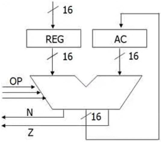
The ALU, the registers, and the interconnecting buses are collectively referred to as datapath. Every bit in datapath is functionally identical. The datapath is competent enough of executing certain operations on data items.
Control Section
The control section is basically referred to as the control unit, whose main goal is to send control signals to the datapath.
Bus: A Bus is defined as a collection of wires or distinct lines which are meant to carry address, data, and control information.
Data Bus: Used for transmission of data. The number of data lines conforms to the number of bits in a word.
Address Bus: It contains the address of the data in the main memory location from where it can be accessed.
Control Bus: It carries control signals like it is used to tell the direction of data transfer and to coordinate the timing of events during the data transfer.
PC (Program Counter): Holds the address of the next instruction
IR (Instruction Register): Holds the executing instruction
Instruction Cache: ‘Fast’ memory where the next instruction comes from Reg[index]
(Register File): It has 32 registers
Arithmetic Logic Unit (ALU): This part is responsible for performing all arithmetic and logical operations.
Data Cache: Data read from or written to ‘fast’ memory
Multiplexer: Multiple inputs selects one output based upon control signal(s)
Single-Cycle Data Path: Each instruction executes in one clock cycle
Multi-Cycle Data Path: Each instruction takes multiple clock cycles
Single-Cycle Data Path
- Every cycle must be of equal length
- The cycle time must be long enough to accommodate the longest instruction.
Multi-Cycle Data Path
- Have the cycle time coincide with the instruction stage time.
- Cycle time = 2 ns (time of longest stage)
- Between stages, we need registers to hold data for the next stage.

- Accumulator: Special register
- One of the inputs to ALU
- The output. of ALU is stored back in the accumulator.
- One-address instructions: Operation and address of one operand
- Another operand and destination is the accumulator register
- AC <– AC op Mem[addr]
- Single address instructions (AC implicit operand)
- Multiple registers: Part of instruction used to choose register operands

Instruction Path
- Program Counter
- Keeps track of program execution
- Address of next instruction to read from memory
- May have an auto-increment feature or use ALU
- Instruction Register
- Current instruction
- Includes ALU operation and address of the operand
- Also holds target of jump instruction
- Immediate operands
- Relationship to Data Path
- PC may be incremented through ALU
- Contents of IR may also be required as input to ALU
CPU Organisation
It is further classified into three types on the basis of ALU Data Paths.
- Stack CPU: In this organisation, ALU operands are required to be in the stack and all the operations are performed on stack memory. basically, Zero address Instruction and One address instructions are used. Example: PUSH A, POP
- Accumulator CPU: In this organisation, One of the operands are required into the main memory and the other is required either in a register or in memory. After the processing, the result will be placed into the main memory. Accumulator becomes the default location here. Example: ADD A
- General Register CPU: In this particular organisation, operands are required to be in registers and after the processing, results gets stored in the main memory. Example: ADD A B, Where A & B registers.
Bus Configurations in the CPU:
- IOP (Input Output Processor): in this configuration, Different buses are used for input-output devices and memory-mapped devices but the control signals and address space is common for both of them. This method is quite costly as it requires the implementation of extra hardware.
- Isolated IO (IO mapped IO): This configuration uses the common buses and common address space for both memory and input-output devices but different control signal are used for both of them. Here, all the signals are active low signals except IO, it will work if the value given to the signal is 0.

- Memory Mapped IO: In this organisation, the buses and control signals are kept common for both memory and input-output devices, but the address space is divided between them. this is more preferred since no need for external hardware.
Memory Interface
Memory
- Separate data and instruction memory: Two address busses, two data busses
- Single combined memory: Single address bus, single data bus
Separate memory
- ALU output goes to data memory input
- Register input from data memory output
- Data memory address from the instruction register
- Instruction register from instruction memory output
- Instruction memory address from the program counter
Single memory
- Address from PC or IR
- Memory output to instruction and data registers
- Memory input from ALU output
Memory Interfacing
This concept is used to integrate the CPU and memory unit. Pins are mapped between the CPU and main memory to get the required functioning.
The latch is used so that single pins can be used for carrying data as well as address i.e, the same lines are used to carry data and address.

Memory Accessing Schemes
- Little Endian Scheme: Data is stored in such a way that lower address location contains lower byte and higher address location contain higher byte.
- Big Endian Scheme: Data is stored in such a way that lower address location contains higher byte and higher address location contain lower byte.
- The default addressing scheme is the Little Endian Scheme.
One-Bus Organization
- CPU registers and the ALU use a single bus to move outgoing and incoming data.
- The bus can handle only a single data movement within one clock cycle.
- This bus organization is the simplest and least expensive.
- It limits the amount of data transfer that can be done in the same clock cycle, which will slow down the overall performance.

Two-Bus Organization
- General-purpose registers are connected to both buses.
- Data can be transferred from two different registers to the input point of the ALU at the same time.
- Two operand operations can fetch both operands in the same clock cycle.

Three-Bus Organization
- Two buses may be used as source buses while the third is used as a destination.
- The source buses move data out of registers (out-bus), and the destination bus may move data into a register (in-bus).
- Each of the two out-buses is connected to an ALU input point. The output of the ALU is connected directly to the in-bus
- Increasing the number of buses will also increase the complexity of the hardware.

Instruction Cycle
- The sequence of operations performed by the CPU during its execution of instructions.
- At the completion of the instruction execution, a test is made to determine whether an interrupt has occurred.
- An interrupt handling routine needs to be invoked in case of an interrupt.

The instruction cycle can be divided into three phases:
- Instruction Fetch: The CPU will read the instruction from the main memory based on the program counter value, which is loaded by the programmer.
- Instruction Execute: It includes the 2 Sub-phases:
- Instruction Decode: in this phase, decoding of the instruction is carried out to know the actual operation to be performed.
- Instruction Execution: After decoding the instruction, the actual execution of the instruction is carried out.
- Interrupt Cycle: After completion for each and every instruction, the CPU checks for any type of interrupt in the system. If there is an interrupt that occurred in the system, then it is serviced and further execution for instruction is carried out.
The basic actions during fetching an instruction, executing an instruction, or handling an interrupt are defined by a sequence of micro-operations.
Addressing Modes
Effective Address Calculation
- Direct Addressing Mode: Effective Address for the operands is present in the instruction itself.
- Immediate Addressing Mode: the instruction itself contains the operand.
- Indirect addressing Mode: Effective address is mentioned at the memory location which is provided in the instruction itself.
- Register Addressing Mode: Operands are present in the register mentioned in the given instruction.
- Indexed Addressing Mode: Effective addresses for operands are calculated by adding the displacement value mentioned in the instruction to the index register.
- PC Relative Mode: Effective address for the operands is calculated by adding the displacement value present in the instruction to the PC register.
Condition Codes/ Program Status Word: The processor keeps track of some information about the results of various operations for use by subsequent conditional branch instructions, by recording the necessary data into individual bits known as condition code flags.
It is further divided into two parts:
- Conditional Flags.
- Control Flags.
Conditional Flags: Important flags of status/condition code register:
- S (Sign) Sets to 1 if the result is negative; otherwise, cleared to 0
- Z (zero) Sets to 1 if the result is 0; otherwise, cleared to 0
- V (overflow) Sets to 1 if an arithmetic overflow occurs; otherwise, cleared to 0
- C (carry) Sets to 1 if carry-out results from the operation; otherwise, cleared to 0
- AC (Auxiliary Carry) Sets to 1 if there is an extra bit from lower nibble to higher nibble, otherwise, it is zero
- P (Parity) Sets to 1 if the no of bits in the result is even; otherwise, cleared to 0
Control Flags: Important control flags are:
- TRAP Flag is set to 1 if single-step program execution is carried out else set to 0.
- Interrupt Flag is set to 0 when interrupts are disabled else set to zero.
- Direction Flag is used to support Auto-Indexed Addressing modes.
|
6 videos|76 docs|52 tests
|

|
Explore Courses for Electronics and Communication Engineering (ECE) exam
|

|


