Diode Circuits | Analog Circuits - Electronics and Communication Engineering (ECE) PDF Download
| Table of contents |
|
| An Overview |
|
| Diode as Rectifier |
|
| Parameter of Full Wave Rectifier |
|
| Regulator |
|

An Overview
In this article, you will find the Study Notes on Simple Diode and Wave shaping Circuits which will cover the topic as Half wave rectifier, Full wave rectifier, Zener Diode, and Regulator.Diode as Rectifier
Any electrical device which offers a low resistance to the current in one direction and a high resistance to the current in the opposite direction is called a rectifier. Such a device is capable of converting a sinusoidal input waveform, whose average value to zero, into a unidirectional (though not constant) waveform, with a non zero average component.
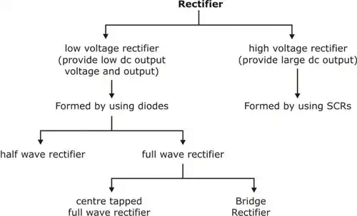
➤ Half wave Rectifier
Half wave rectifier will rectify only half position of input either positive or negative. The basic circuit for half wave rectification is shown in figure 1.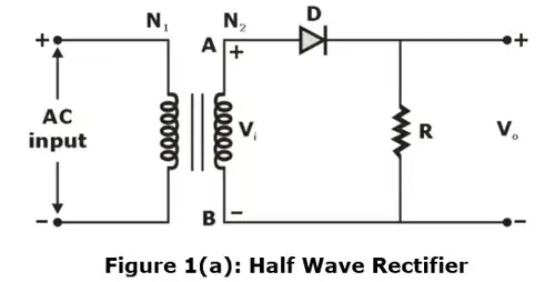 AC voltage across the secondary winding AB changes polarity after every cycle during the positive half cycle of input ac voltage, end a becomes positive w.r.t end B. This makes the diode forward biased and hence it conducts current.
During the negative half cycle end A is negative w.r.t end B. Under this condition, the diode is reverse biased and it conduct no current.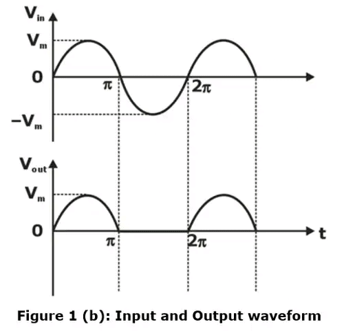
Parameter of output waveform
A. output DC voltage or current
B. output rms voltage or current
C. Ripple factor
D. Peak inverse voltage
E. Efficiency
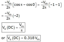
(a) Output DC voltage or current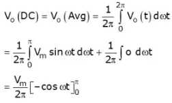
(b) Output rms voltage or current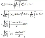
(c) Ripple factor
A measure of the fluctuating components is given by the ripple factor which is defined as
γ = rms value of alternating components of wave/Average value of wave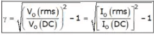
Which is sometime approximated as,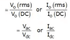
Ripple factor of half wave rectifier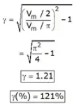
(d) Peak inverse voltage (PIV)
The maximum reverse voltage the diode can with stand without breakdown.
PIV = Vm
(e) Current handling capability of a diode
It is maximum current, that should not exceed otherwise breakdown occurs.
(f) Efficiency
It is a measure of the ability of a rectifier to convert AC power into dc power.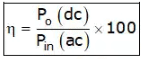
= (output dc power/input ac power)x100
P0(DC) = V.I = V0(DC).I0(DC)
Pin(AC) = Vrms . Irms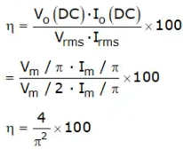
η = (4/π2)x100
= 0.405 x 100
η = 40.5%
Conclusion
- It rectifies one half of the input AC signal
- V0(dc) = Vm/π = 0.318Vm
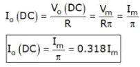
- I0(dc) = Im/π = 0.318Im
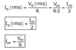
- V0(rms) = Vm/2
- I0(rms) = Im/2
- Im = Vm/R
- γ = 1.21
- PIV = Vm
- Time period = T = 2n
Disadvantage of half wave rectifier
(i) Vo (DC) = 0.318 Vm
Output DC voltage is only 31.8% of peak input voltage Vm
(ii) η = 40.5%
Efficiency is only 40.5%, that is only 40.5% is converted into DC remaining will be lost.
➤ Full Wave Rectifier
In full wave rectification, current flows through the load in the same direction for both half cycles of input ac voltage. This can be achieved with two diodes working alternatively. For the positive half cycle of input voltage, one diode supplies current to load and for the negative half cycle, the other diode does so; current being always in the same direction through the load.
The following two circuits are used for full wave rectifier
(a) Centre- tap full wave rectifier
(b) Full wave bridge rectifier
(a) Centre-Tapped Full-wave Rectifier
The circuit of a centre-tapped full-wave rectifier is shown in Figure 2(a). This circuit is seen to comprise two half-wave circuits which are so connected that conduction takes places through one diode during one half of the power cycle and through other diode during the second half of the power cycle.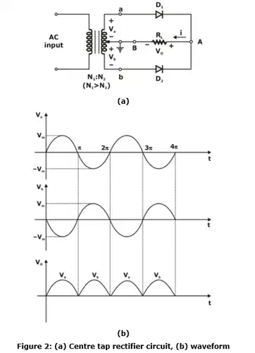
In this rectifier centre-tapped step down transformer has been used, in which secondary winding is divided into two halves, each half having equal number of turns. In N1 : N2 centre-tapped transformer, primary winding has N1 turns and each half of secondary winding has N2 turns.
When centre terminal of secondary winding is grounded, voltage at nodes a and b will have equal magnitude but opposite sign;
i.e., Vb = – Va
if Va = Vm sinα
then Vb = – Vm sinα
Operation
- When 0 < α < π
Then Va is positive so diode D1 is forward biased and in this case Vb is negative so diode D2 is reverse biased. As diode D1 is in conduction mode so node ‘a’ gets shorted to RL therefore Vo= Va - When π < α < 2π
Then Va is negative so diode D1 is reverse biased and Vb is positive so diode D2 is forward biased. As diode D2 is in conduction mode so node ‘b’ gets shorted to RL therefore Vo= Vb
Parameter of Full Wave Rectifier
A. output dc componentB. output RMS value
C. Ripple factor
D. Peak converse voltage
E. Efficiency
(A) Output DC voltage
(C) Ripple factor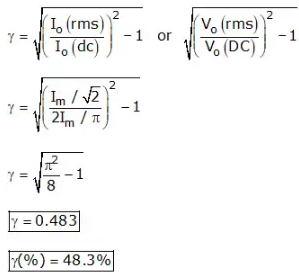
(D) Efficiency
η = (output DC power/input AC power)x100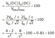
η = 81%
(E) Peak inverse voltage
PIV = 2Vm
Conclusion
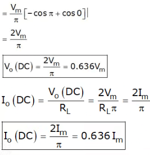
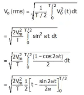
- V0(DC) = 2Vm/π = 0.636Vm
- Io(DC) = 2Im/π = 0.636Im
- γ = 0.483
- η = 81%
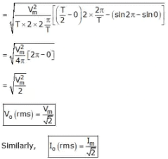
- Vrms = Vm/√2
- Irms = Vm/√2
- Time period, T = T/2 = n
(b) Bridge Rectifier
The full wave rectifier circuit requires a centre-tapped transformer where only one half of the total ac voltage of the transformer secondary winding is utilized to convert into dc output. Now consider a different configuration of full wave rectifier circuit, called bridge rectifier, where entire AC voltage of the transformer secondary is used to convert into DC voltage.
Figure 3 shows a bridge rectifier circuit. There are four diodes D1, D2, D3 and D4 which form the four arms of the bridge. AC from transformer secondary is fed to two corners and the load resistance RL is connected to other two corners.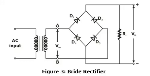
During positive half-cycle of input, point A is positive, diodes D1 and D3 are forward biased and diodes D2, D4 are reverse biased then, the current flows through diodes D1, the load RL and through diode D3 back to the negative polarity of the transformer secondary. During negative half cycle of input point B is more positive than point A, thus diode D2, D4 are forward biased and diode D1 and D3 are reversed biased, then the direction of current flow will be through diode D2 load RL and diode D4. In both case the current flowing through resistor RL is in same direction, thus it is unidirectional current and we obtain full wave rectification.
Regulator
- The most important property for an ideal power supply is to maintain a constant voltage at the output terminals for all operating conditions.
- But practically there is a drop-in output terminal voltage of the power supply as the load current increases, so we require to regulate the power at optimum level using a voltage regulator.
(a) Performance Parameters of a Good Voltage Regulator
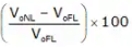
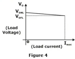
- Load Regulation Factor
It is the change in the load voltage from no load to full load.
% Load Regulation =
- Line Regulation Factor
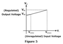
It is the effect of variations in the supply voltage causing variations in the output voltage of the regulator.
V01 is the output voltage at the maximum input voltage while V02 is the output voltage at the minimum input voltage.
Temperature Coefficient of the output voltage
It is the effect of temperature over the performance of the regulator. It is defined as Ideally it should be zero. - Output Resistance
For voltage regulation, multiple units of regulator might be cascaded. Thus, to make the coupling smooth the output resistance of the regulator should as low as possible, ideally zero. - Maximum Dissipated Power
The maximum power dissipation by the Zener diode should be as low as possible.

 Ideally it should be zero.
(b) Zener Diode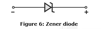
- Zener diode is a special purpose diode designed to operate under reverse bias in the breakdown region.
- A Zener diode has higher doping than conventional diodes
- In a Zener diode the depletion layer is very thin and electric field strength at the junction is very high even for a small reverse voltage.
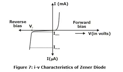
(c) Application of Zener Diode as a Voltage Regulator
- At the instant when the applied reverse biased voltage on the Zener diode is equal to the Zener breakdown voltage, further increase in reverse voltage makes the electric field at the p-n junction significantly high.
- The electric field is high enough to pull the electrons that are beyond the junction on the n-side towards the p-side, significantly increasing the current.
- The increased current allows a wide range of current to flow through the diode in the breakdown region such that the reverse voltage has no significant change.
(d) Equivalent Circuit of Zener Diode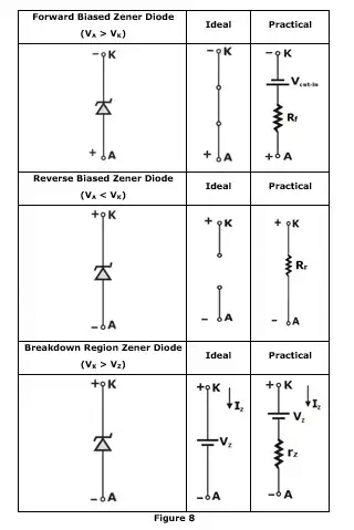
(e) Drawbacks of Zener Voltage Regulators
- The Zener diode can be operated as a voltage regulator within a limited range of reverse current.
- Power dissipation for the Zener diode is practically large enough to affect the efficiency of the device.
- The output resistance of a Zener voltage regulator is practically not as low as desired for the cascading operation.
|
3 videos|34 docs|64 tests
|
FAQs on Diode Circuits - Analog Circuits - Electronics and Communication Engineering (ECE)
| 1. What is the function of a diode as a rectifier? |  |
| 2. What are the parameters of a full-wave rectifier? | |
| 3. How does a regulator diode circuit work? | |
| 4. What is the role of diodes in electronics and communication engineering? | |
| 5. What are some common applications of diodes in electronics? | |


Top Courses for Electronics and Communication Engineering (ECE)
Diode Circuits | Analog Circuits - Electronics and Communication Engineering (ECE)
,study material
,Exam
,Previous Year Questions with Solutions
,MCQs
,Diode Circuits | Analog Circuits - Electronics and Communication Engineering (ECE)
,Summary
,past year papers
,practice quizzes
,Sample Paper
,ppt
,Diode Circuits | Analog Circuits - Electronics and Communication Engineering (ECE)
,mock tests for examination
,shortcuts and tricks
,Semester Notes
,Important questions
,Objective type Questions
,Extra Questions
,Viva Questions
,video lectures
,Free
;


Diode Circuits Free PDF Download
Importance of Diode Circuits
Diode Circuits Notes
Diode Circuits Electronics and Communication Engineering (ECE) Questions
Study Diode Circuits on the App
|
© EduRev
|
Education Revolution
|


|


