Frequency Response | Analog Circuits - Electronics and Communication Engineering (ECE) PDF Download
Frequency Response of Amplifiers
➤ Introduction
- Amplifiers do not have the same gain at all frequencies.
- An amplifier designed for radio frequencies will amplify a band of frequencies above about 100kHz but will not amplify the lower frequency audio signals.
- In each case the amplifier has a particular frequency response, being a band of frequencies where it provides adequate amplification, and excluding frequencies above and below this band, where the amplification is less than adequate.
➤
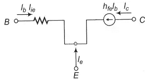
Hybrid Equivalent Circuit for a Transistor- Any single stage transistor amplifier, whether CB, CE or CC may be put in a standard form for small signal analysis so as to be able to identify Vg, Rg, and RL as well as the transistor’s input and output terminals.
- The hybrid equivalent circuit for a transistor consists of a Thevenin equivalent circuit at the input and a Norton equivalent circuit at the output.
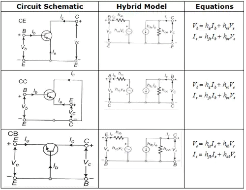
- The equations relating the input and output voltages and currents in a transistors small signal equivalent circuit are given by

- hi = Input impedancehr = Reverse voltage ratio
- hf = Forward current transfer ratio
- h0 = Output admittance
- where, hi, hr, hf and h0 are the h-parameters and have a second subscript of b, e or c according to the amplifier in question.
- The h-parameters may be obtained from the transistor’s characteristic curve or may be measured experimentally by using changes in current and voltage levels to stimulate AC conditions.
- Typical h-parameter values for CB, CE and CC connections are shown in tables given below and are all dependent upon the collector current.
Typical h-parameters for A 2N3391 Silicon Transistor, Evaluated at Ic= 1mA, VCE =5V, f=1kHz, and TA=25 degree Centrigrade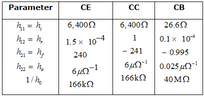
Typical h-parameters for A2N404 Germanium Transistor, Evaluated at Ic = 1mA, VCE = 6V, f = 1kHz, and TA = 25 degree Centrigrade.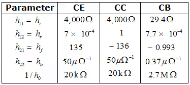
- If the h-parameters are given for one type of amplifier connection but are required for another type, the approximate conversion formulae in may be used.
Approximate Conversion Formulae for Transistor h-parameters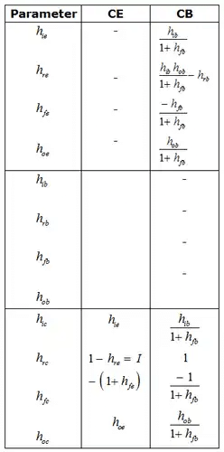
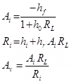
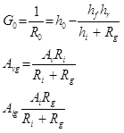
- Knowing the h-parameters for a transistor, the values for Ai, Ri, Av, Ro Avg and Aig may be obtained using the exact equations in the table by using a second subscript appropriate to the amplifier being analyzed. The value of Rg and RL are also necessary.
- Exact equations for the small signal analysis of transistor amplifiers


Using a transistor’s h-parameters, it is possible to dually match Rg and PL for the Maximum Available Power Gain (MAG) from the transistor, Equations

- Where Δh= hi ho - ho hf
Circuit schematic hybrid model and V-I, h-parameter equations for the CE, CC and CB amplifier connections
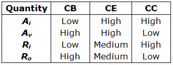
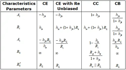
- A transistor amplifier’s characteristics are very dependent upon the values used for Rg and RL, but generally speaking, the characteristics may be summarized as in the given ahead.
Comparison between CB, CE, CC
Approximate equations for Ai, Ri, Av and R0 in terms of CE h-parameter are shown in table and are valid if, hoeRL ≤ 0.1
Approximate hybrid equivalent circuit at low frequencies, when at low frequencies, when hoeRL ≤ 0.1 - hoe=he=0
- Approximate equations for Ai, Ri, Av and R0 for CB, CE or CC amplifiers, given in terms of Ce h-parameters. To be used only when hoe RL or hoe he<=0.1 is given below

➤
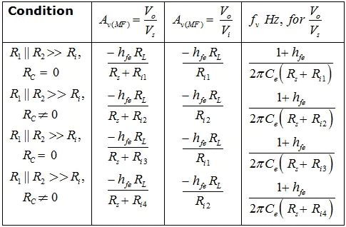
Low-Frequency Response of Amplifier- The value of the emitter bypass capacitor in a single stage CE amplifier must be very large to provide a low value for the lower 3-dB frequency. f1 equations for f1 for different circuit conditions are summarized in the table.
- Summary of the approximate equations for mid frequency voltage gain and lower 3-dB frequency f1. For various circuit conditions:

- The electrolyte losses in the emitter bypass capacitor affect the low-frequency response some what but have a significant effect on mid frequency gain.
- Low-frequency response is also affected by the size of the coupling capacitors, as shown by

Where R'i is the effective input resistance to the amplifier. - The overall mid frequency voltage gain of an amplifier consisting of cascaded CE stages is the product of the gains of all of the stages. But the overall current gain must take into account the load and be biasing resistors, along with the transistor input impedances.
- Analysis of cascaded stages generally proceeds from the last stage back towards the input, by determining Ai, Ri and Av in that order.
- The overall low-frequency response, f1(n) for n cascaded stages each having the same value of f1 given by

which shows that the low-frequency response is poorer than for a single stage. - The ability of an amplifier to handle a square wave signal is measured by the sag and is related to the amplifiers lower 3-dB frequency, f1 by

where f is the frequency of the square wave. To provide a low Sag requires a very low value for f1. - Cascaded transformer coupled amplifiers designed for maximum power transfer conditions have equal current and voltage gains given by

- The lower 3-dB frequency f1, for a transformer coupled amplifier, is restricted by the transformer’s primary inductance Lp, as given by

Where R is the effective portion of the transistor’s load and output resistance in parallel with Lp. - In order for a transformer coupled amplifier to handle a pulse of duration td with less than a given amount of Sag, the transformer must have a minimum primary inductance is given by

➤
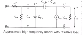
High-Frequency Response of Amplifiers- The hybrid-π model of a transistor at high frequencies includes the capacitive effects of the p-n junction and involves a base spreading resistance that creates a virtual base.
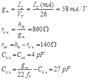
- The transistor’s high-frequency parameters are given in equations below and include the transistors transconductance.
- The parameters for the approximate hybrid-π model may be obtained from the following equations. (Numerical values shown are for 1 2N 2218 silicon transistor with:


Cb’c is usually given in the transistor manual as Cob and is the CB open circuit output capacitance Cb’e may be given the manufacturer or it may be calculated using the equation given, ft is the frequency at which the CE short circuit current gain drops to unity. - The transistor’s short circuit current gain varies with frequency and is characterized by the α cut-off and β cut off frequencies, where the current gain drops by 3 dB from the value at mid frequencies in a CB and CE connection respectively.
- Important high-frequency characteristics of a transistor are ft, the gain bandwidth product and are defined to be the frequency at which a common emitter’s short circuit current gain drops to unity.
- Cascaded CE stages operating at high frequency have a reduced overall bandwidth given by

where n is the number of stages and f2 is the bandwidth of each stage - The ability of an amplifier to reproduce a square wave input with a low rise time, tr, is directly proportional to the bandwidth f2. That is
tr = 0.35/f2 - When a transistor is operated at high frequencies with a resistive load, the collector to base junction capacitance appears as an enlarged value of capacitance at the input, thus reducing voltage and current gain below the values expected at the α and β cut-off.
- The high-frequency response of a transformer coupled amplifier is usually limited entirely by the transformer’s leakage inductance and distributed capacitance, which creates a series resonant effect.
- Transistor noise is usually measured as a spot noise figure, NF or as the average noise figure NF, with typical values between 0.5 and 5 dB depending upon the source resistance, collector current, and frequency.
The document Frequency Response | Analog Circuits - Electronics and Communication Engineering (ECE) is a part of the Electronics and Communication Engineering (ECE) Course Analog Circuits.
All you need of Electronics and Communication Engineering (ECE) at this link: Electronics and Communication Engineering (ECE)
|
3 videos|33 docs|64 tests
|
FAQs on Frequency Response - Analog Circuits - Electronics and Communication Engineering (ECE)
| 1. What is the frequency response of an amplifier? |  |
Ans. The frequency response of an amplifier refers to its ability to pass or amplify signals of different frequencies. It indicates how the gain or output of the amplifier varies with the input frequency.
| 2. Why is frequency response important in amplifier design? |  |
Ans. Frequency response is crucial in amplifier design as it determines the range of frequencies that can be accurately amplified. It helps in maintaining the fidelity of the signal and ensures that the amplifier does not introduce distortion or attenuate certain frequencies.
| 3. How is frequency response measured in amplifiers? |  |
Ans. Frequency response in amplifiers is measured using a frequency sweep test. A signal generator is used to generate a range of frequencies, and the output of the amplifier is then measured for each frequency using an oscilloscope or spectrum analyzer. The results are plotted on a graph to visualize the frequency response.
| 4. What is the significance of the bandwidth in amplifier frequency response? |  |
Ans. The bandwidth of an amplifier represents the range of frequencies over which the amplifier can operate effectively. It is determined by the lower and upper cutoff frequencies, beyond which the gain starts to decrease. A wider bandwidth indicates a more versatile and capable amplifier.
| 5. How can the frequency response of an amplifier be improved? |  |
Ans. The frequency response of an amplifier can be improved by using techniques like negative feedback, careful component selection, and proper circuit design. Negative feedback helps in stabilizing the gain across different frequencies, while selecting high-quality components and designing a well-matched circuit can minimize distortions and improve overall performance.

|
Explore Courses for Electronics and Communication Engineering (ECE) exam
|

|
Signup for Free!
Signup to see your scores go up within 7 days! Learn & Practice with 1000+ FREE Notes, Videos & Tests.
Related Searches

