Gate Questions on Semiconductors | Electronic Devices - Electronics and Communication Engineering (ECE) PDF Download
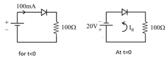
Q.1. An ideal p-n junction diode in series with a 100 Ω resistance is forward biased such that the forward current flowing through the diode is 100 mA. If voltage across this circuit is instantaneously reversed to 20 V at time instant t = to, then the reverse current flowing through the diode at time instant t = to is approximately given by
(a) 0 mA
(b) 200 mA
(c) 100 mA
(d) 2 mA
Correct Answer is Option (b)
If a diode is conducting in forward bias and immediately switched to reverse bias voltage , the diode will allow to flow the current in reverse bias for short time so that the forward voltage bleeds off, (or we can say for the time which diode takes to be in complete reverse bias, it act as a short circuit). This is called reverse recovery time.
I = 20/100
= 200mA.
Q.2. An N-type semiconductor having uniform doping is biased as shown in the figure. If EC is the lowest energy level of the conduction band, Er is the highest energy level of the valance band and EF is the Fermi level, which one of the following represents the energy band diagram for the biased N-type semiconductor?
(a)
(b) 
(c) 
(d) 
Correct Answer is Option (d)
In N-type, Semiconductor Ef lies near to the conduction Band and since it is positively biased on right side so energy band diagram will be tilted downwards on right side, hence option D is the correct answer.
Q.3. Consider a silicon sample doped with ND = 1 × 10¹⁵ /cm3 donor atoms. Assume that the intrinsic carrier concentration ni = 1.5 × 10¹⁰ /cm3. If the sample is additionally doped with NA = 10 × 1018 /cm3 acceptor atoms, the approximate number of electrons/cm3 in the sample, at T = 300 K, will be _________________.
(a) 22.52
(b) 245.2
(c) 255.2
(d) 265.2
Correct Answer is Option (a)
Q.4. The cut-off wavelength (in μm) of light that can be used for intrinsic excitation of a semiconductor material of bandgap Eg = 1.1 eV is ________.
(a) 0.85 μm
(b) 1.125 μm
(c) 1.450 μm
(d) 2.250 μm
Correct Answer is Option (b)
Q.5. In the figure in (pi) is plotted as a function of 1/T, where (pi) the intrinsic resistivity of silicon, T is the temperature, and the plot is almost linear.
 The slope of the line can be used to estimate
(a) Band gap energy of silicon (Eg)
(b) Sum of electron and hole mobility in silicon (μn + μp)
(c) Reciprocal of the sum of electron and hole mobility in silicon (μn + μp) -1
(d) Intrinsic carrier concentration of silicon
Correct Answer is Option (a)
The given plot is between ln(Pi) and 1/T.As temperature (T) increases Energy gap Eg decreases Due to decrease in Eg electron hole pair generation increase. So conductivity (σ) increases. This can be represented is short as
Plot is linear
So the slope can be used to determine the band gap (Eg)
The book of S.M. Sze contains the plot of intrinsic carrier densities for Si and GaAs as 1/T
The larger the band gap the smaller the intrinsic carrier density.
Q.6. A silicon bar is doped with donor impurities ND = 2.25 x 10¹⁵ atoms / cm3. Given the intrinsic carrier concentration of silicon at T = 300 K is ni = 1.5 x 1010 cm-3. Assuming complete impurity ionization, the equilibrium electron and hole concentrations are
(a) 
(b) 
(c) 
(d) 
Correct Answer is Option (d)
Given the concentration of donor impurities,
ND = 2.25 x 10¹⁵ atoms/cm3
Intrindic carrier concentration,
ni = 1.5 x 1010 cm-3
Since, we haveND >> ni
Since complete ionization taken place,
n0 = ND = 2.25 x 1015 cm-3
Hence, using mass action law, we obtain the hole concentration as
Q.7. When the optical power incident on a photodiode is 10μW and the responsivity is 0.8A/W, the photocurrent generated (inμA) is ________.
(a) 2
(b) 4
(c) 6
(d) 8
Correct Answer is Option (d)
The responslvity is define as
where
P is optical power incident on photodiode.
1P is photocurrent
Ip = PR
= (10 pW)(0.8 A/W)
= 10 x 10-6 x 0.8
= 8 x 10⁻⁶ A
Ip = 8μ A
Q.8. Two sequences x1 [n] and x2 [n] have the same energy. Suppose x1[n] = a 0.5n u[n], where a is a positive real number and u[n] is the unit step sequence. Assume
Then the value of a is__________.
Ans. 1.5
x1[n]= -(0.5)nu[n]
Energy of signal x1[n] is
Again, x2[n] =
So, energy of signal x2[n] is
Given that
Energy of signal x1[n] = Energy of signal x2 [n]
Since α is a positive real number, so we have
α = 1.5
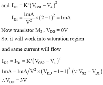
Q.9. In the circuit shown, both the enhancement mode NMO transistors have the following characteristics: kn = mn Cox (W/L) = 1 mA/V2; VTN= 1V. Assume that the channel length modulation parameter l is zero and body is shorted to source. The minimum supply voltage VDD (in volts) needed to ensure that transistor M1 operates in saturation mode of operation is _________ 
Ans. 3V
Given Circuit is Shown below
Q.10. The current in an enhancement mode NMOS transistor biased in saturation mode was measured to be 1 mA at a drain-source voltage of 5 V. When the drain-source voltage was increased to 6V while keeping gate-source voltage same, the drain current increased to 1.02 mA. Assume that drain to source saturation voltage is much smaller than the applied drain-source voltage. The channel length modulation parameter λ (in V–1) is ______.
Ans. 0.022 v-1
Q.11. The injected excess electron concentration profile in the base region of an npn BJT, biased in the active region, is linear, as shown in the figure. If the area of the emitter-base junction is 0.001 cm2, in the base region and depletion layer widths are negligible, then the collector current Ic (in mA). at room temperature is __________
 (Given: thermal voltage VT = 26 mV at room temperature, electronic charge
 )
)
Ans. 6.6 mA
Q.12. Consider an n-channel metal oxide semiconductor field effect transistor (MOSFET) with a gate-to source voltage of 1.8 V. Assume that (W/L) = 4, μN COX = 70 x 10-6 AV-2, the threshold voltage is 0.3V, and the channel length modulation parameter is 0.09 V-1. In the saturation region, the drain conductance (in micro siemens) is _______.
Ans. 28.35
The equation of current in saturation is given by
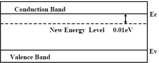
Q.13. A small percentage of impurity is added to an intrinsic semiconductor at 300 K. Which one of the following statements is true for the energy band diagram shown in the following figure?
 (a) Intrinsic semiconductor doped with pentavalent atoms to form n-type semiconductor
(b) Intrinsic semiconductor doped with trivalent atoms to form n-type semiconductor
(c) Intrinsic semiconductor doped with pentavalent atoms to form p-type semiconductor
(d) Intrinsic semiconductor doped with trivalent atoms to form p-type semiconductor
Correct Answer is Option (a)
Pentavalent impurity when introduced in intrinsic semiconductor then a new diecrete energylevel called Donor energy level is created just below the conduction band
Q.14. For a particular intensity of incident light on a silicon pn junction solar cell, the photocurrent density (JL) is 2.5 mA/cm2 and the open-circuit voltage (VOC) is 0.451 V. Consider thermal voltage (VT) to be 25mV. If the intensity of the incident light is increased by 20 times, assuming that the temperature remains unchanged. Voc (in volts) will be__________.
Ans. 0.525 V
Open circuit voltage of solar cell is given by.
Where, JL = Photo current density.JJ = Reverse saturation current density.
VT = Thermal voltage.
When intensity of the incident light is increased by 20 times then
Given: Temperature is constant, so
New open circuit voltage.
From equation (i),= 0.451+ (0.025 In 20) = 0.525 V
Q.15. A junction is made between p- Si with doping density NA1 = 1015 cm-3 and p Si with doping density NA2 =1017 cm-3.
Given: Boltzmann constant k= 1.38 x 10⁻²³ J.K-1 , electronic charge q= 1.6 x 10⁻¹⁹ C.
Assume 100% acceptor ionization.
At room temperature (T= 300K), the magnitude of the built-in potential (in volts, correct to two decimal places) across this junction will be ____________.
Ans. 0.119 V
As per details given in Question
Q.16. An n+-n Silicon device is fabricated with uniform and non-degenerate donor doping concentrations of ND1 = 1 × 1018 cm-3 and ND2 = 1 × 1015 cm-3 corresponding to the n+ and n regions respectively. At the operational temperature T, assume complete impurity ionization, kT/q = 25 mV, and intrinsic carrier concentration to be ni = 1 × 1010 cm-3. What is the magnitude of the built-in potential of this device?
(a) 0.748 V
(b) 0.460 V
(c) 0.288 V
(d) 0.173 V
Correct Answer is Option (d)

Q.17. A bar of Gallium Arsenide (GaAs) is doped with Silicon such that the Silicon atoms occupy Gallium and Arsenic sites in the GaAs crystal. Which one of the following statement is true?
(a) Silicon atoms act as p-type dopants in Arsenic sites and n-type dopants in Gallium sites
(b) Silicon atoms act as n-type dopants in Arsenic sites and p-type dopants in Gallium sites
(c) Silicon atoms act as p-type dopants in Arsenic as well as Gallium sites
(d) Silicon atoms act as n-type dopants in Arsenic as well as Gallium sites
Correct Answer is Option (a)
- Substituting a Gallium site by a si atom produces a free electron so n-type
- Substituting an Arsenic site by a si atom produces a hole
so p-type.
|
21 docs|29 tests
|

|
Explore Courses for Electronics and Communication Engineering (ECE) exam
|

|


 = 0.451+ (0.025 In 20) = 0.525 V


