Heterojunction Devices - Semiconductor Devices, CSIR-NET Physical Sciences | Physics for IIT JAM, UGC - NET, CSIR NET PDF Download

A heterojunction is the interface that occurs between two layers or regions of dissimilar crystalline semiconductors. These semiconducting materials have unequal band gaps as opposed to a homojunction. It is often advantageous to engineer the electronic energy bands in many solid-state device applications, including semiconductor lasers, solar cells and transistors ("heterotransistors") to name a few. The combination of multiple heterojunctions together in a device is called a heterostructure, although the two terms are commonly used interchangeably. The requirement that each material be a semiconductor with unequal band gaps is somewhat loose, especially on small length scales, where electronic properties depend on spatial properties. A more modern definition of heterojunction is the interface between any two solid-state materials, including crystalline and amorphous structures of metallic, insulating, fast ion conductor and semiconducting materials.
In 2000, the Nobel Prize in physics was awarded jointly to Herbert Kroemer (University of California, Santa Barbara, California, USA) and Zhores I. Alferov (Ioffe Institute, Saint Petersburg, Russia) for "developing semiconductor heterostructures used in high-speed- and opto-electronics".
Manufacture and applications
Heterojunction manufacturing generally requires the use of molecular beam epitaxy (MBE)[1] or chemical vapor deposition (CVD) technologies in order to precisely control the deposition thickness and create a cleanly lattice-matched abrupt interface.
Despite their expense, heterojunctions have found use in a variety of specialized applications where their unique characteristics are critical:
Lasers: Using heterojunctions in lasers was first proposed[2] in 1963 when Herbert Kroemer, a prominent scientist in this field, suggested that population inversion could be greatly enhanced by heterostructures. By incorporating a smaller direct band gap material like GaAs between two larger band gap layers like AlAs, carriers can be confined so that lasing can occur at room temperature with low threshold currents. It took many years for the material science of heterostructure fabrication to catch up with Kroemer's ideas but now it is the industry standard. It was later discovered that the band gap could be controlled by taking advantage of the quantum size effects in quantum well heterostructures. Furthermore, heterostructures can be used as waveguides to the index step which occurs at the interface, another major advantage to their use in semiconductor lasers. Semiconductor diode lasers used in CD and DVD players and fiber optic transceivers are manufactured using alternating layers of various III-V and II-VI compound semiconductors to form lasing heterostructures.
Bipolar transistors: When a heterojunction is used as the base-emitter junction of a bipolar junction transistor, extremely high forward gain and low reverse gain result. This translates into very good high frequency operation (values in tens to hundreds of GHz) and low leakage currents. This device is called a heterojunction bipolar transistor (HBT).
Field effect transistors: Heterojunctions are used in high electron mobility transistors (HEMT) which can operate at significantly higher frequencies (over 500 GHz). The proper doping profile and band alignment gives rise to extremely high electron mobilities by creating a two dimensional electron gas within a dopant free region where very little scattering can occur.
Energy band alignment
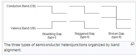
The three types of semiconductor heterojunctions organized by band alignment.
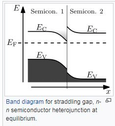
Band diagram for straddling gap, n-n semiconductor heterojunction at equilibrium.
The behaviour of a semiconductor junction depends crucially on the alignment of the energy bands at the interface. Semiconductor interfaces can be organized into three types of heterojunctions: straddling gap (type I), staggered gap (type II) or broken gap (type III) as seen in the figure.[citation needed] Away from the junction, the band bending can be computed based on the usual procedure of solving Poisson's equation.
Various models exist to predict the band alignment.
The simplest (and least accurate) model is Anderson's rule, which predicts the band alignment based on the properties of vacuum-semiconductor interfaces (in particular the vacuum electron affinity). The main limitation is its neglect of chemical bonding.
A common anion rule was proposed which guesses that since the valence band is related to anionic states, materials with the same anions should have very small valence band offsets. This however did not explain the data but is related to the trend that two materials with different anions tend to have larger valence band offsets than conduction band offsets.
Tersoff[3] proposed a gap state model based on more familiar metal-semiconductor junctions where the conduction band offset is given by the difference in Schottky barrier height. This model includes a dipole layer at the interface between the two semiconductors which arises from electron tunneling from the conduction band of one material into the gap of the other (analogous to metal-induced gap states). This model agrees well with systems where both materials are closely lattice matched[4] such as GaAs/AlGaAs.
The 60:40 rule is a heuristic for the specific case of junctions between the semiconductor GaAs and the alloy semiconductor AlxGa1−xAs. As the x in the AlxGa1−xAs side is varied from 0 to 1, the ratio
 tends to maintain the value 60/40. For comparison, Anderson's rule predicts
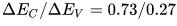 for a GaAs/AlAs junction (x=1).[5][6]
The typical method for measuring band offsets is by calculating them from measuring exciton energies in the luminescence spectra.[6]
Effective mass mismatch at heterojunctions
When a heterojunction is formed by two different semiconductors, a quantum well can be fabricated due to difference in band structure. In order to calculate the static energy levelswithin the achieved quantum well, understanding variation or mismatch of the effective mass across the heterojunction becomes substantial. The quantum well defined in the heterojunction can be treated as a finite well potential with width of  . Addition to that, in 1966, Conley et al.[7] and BenDaniel and Duke[8] reported boundary condition for the envelope function in quantum well, known as BenDaniel-Duke boundary condition. According to them, the envelope function in fabricated quantum well must satisfy boundary condition which states
 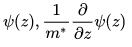 are both continuous in interface regions.
FAQs on Heterojunction Devices - Semiconductor Devices, CSIR-NET Physical Sciences - Physics for IIT JAM, UGC - NET, CSIR NET
| 1. What is a heterojunction device? |  |
| 2. What are the advantages of heterojunction devices over homojunction devices? | |
| 3. How are heterojunction devices used in optoelectronics? | |
| 4. Can you explain the concept of band alignment in heterojunction devices? | |
| 5. What are some examples of heterojunction devices? | |


past year papers
,Previous Year Questions with Solutions
,Summary
,shortcuts and tricks
,mock tests for examination
,practice quizzes
,Free
,Important questions
,CSIR NET
,Sample Paper
,ppt
,Heterojunction Devices - Semiconductor Devices
,CSIR-NET Physical Sciences | Physics for IIT JAM
,Exam
,CSIR-NET Physical Sciences | Physics for IIT JAM
,CSIR-NET Physical Sciences | Physics for IIT JAM
,video lectures
,Extra Questions
,Objective type Questions
,UGC - NET
,Viva Questions
,MCQs
,study material
,Heterojunction Devices - Semiconductor Devices
,Semester Notes
,CSIR NET
,Heterojunction Devices - Semiconductor Devices
,CSIR NET
,UGC - NET
,UGC - NET
;


Heterojunction Devices - Semiconductor Devices, CSIR-NET Physical Sciences Free PDF Download
Importance of Heterojunction Devices - Semiconductor Devices, CSIR-NET Physical Sciences
Heterojunction Devices - Semiconductor Devices, CSIR-NET Physical Sciences Notes
Heterojunction Devices - Semiconductor Devices, CSIR-NET Physical Sciences Physics Questions
Study Heterojunction Devices - Semiconductor Devices, CSIR-NET Physical Sciences on the App
|
© EduRev
|
Education Revolution
|


|


