Junction Theory & Different Types of Diodes & Their Characteristics - 2
Diode Resistance
The static resistance R of a diode is defined as the ratio V/I of the voltage to the "Current Typical values for a silicon planar epitaxial diode are VF = 0.8V at IF - 10mA (corresponding to RF = 80Ω) and IR = 0.1μA at VR = 50V (corresponding to RR = 500M).
For small signal operation the dynamic, or incremental, resistance r is an important parameter and is defined as the reciprocal of the slope of the volt-ampere characteristic, r = dV/dl. The dynamic resistance is not a constant, but depends upon the operating voltage.
The dynamic conductance g = 1/r is

for |V/η)VT| >> 1, g is small and r is very large.
For forward bias, I >> I0, and r is given by
r ≈ (ηVT) /I ....(15)
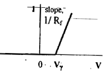
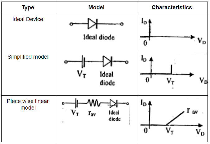
 The piecewise linear characterization of a semiconductor diode.
For an avalanche diode, Vy = Vz, and Rf is the dynamic resistance in the breakdown region.

Transition or Space charge (Or Depletion Region) Capacitance (CT)
The parallel layers of oppositely charged immobile ions on the two sides of the junction-form the transition capacitance, Cr, which is given by
CT = (εA)/W
Where ε(= ε0εr) is the permittivity of the material, A is the cross-sectional area of the junction and W is the width of the depletion layer over which the ions are uncovered.
The net charge must be zero across the depletion region will satisfy the condition
NAWp = NDWn .....(16)
Where
NA = acceptor concentration ; ND-donor concentration;
Wp = width of the depletion region in p-side;
Wn = width of the depletion region in n-side;
The effective barrier potential across the junction is
VB= (qNA W2) / 2ε ....(17)
if NA<< ND, then WP>>Wn
The total depletion width, W is given by
 ....(18)
where,
VB = (V0 - V), V is the applied voltage and V0 is the barrier potential, or the contact
potential.
- When no external voltage is applied, i.e., V = 0, the width of the depiction region of a p n junction diode is of the order of 0.5 microns. The movement of majority carriers across the junction causes opposite charges to be stored at this distance W apart. This depletion region acts as a dielectric between the two conducting p- and n-regions. Therefore, these regions act as a parallel plate capacitor whose transition capacitance CT is approximately 20 pF with no external bias.
- When forward bias +V is applied, the effective barrier potential, VB = [V0 - (+V)|, is lowered and hence the width of the depletion region W decreases and CT increases. Under reverse bias condition, the majority carriers move away from the junction, thereby uncovering more immobile charges. Now the effective barrier potential,
VB = |V0 - (-V)l, is increased and hence, W increase with reverse voltage and CT decreases correspondingly. - The values of CT range from 5 to 200 pF, the larger rallies being for the high power diodes. This property of voltage variable capacitance with the reverse bias appears in varactors, Vari-caps or volta-caps.
Diffusion (Or Storage) Capacitance (Cn)
The capacitance that exists in a forward biased junction is called a diffusion or storage capacitance (CD), whose value is usually much larger than CT, which exists in a reverse-biased junction. This is also defined as the rate of change of-injected charge with applied voltage, i.e., CD - (dQ/dV), where dQ represents the change in the number of minority camel's stored outside the depletion region when a change in voltage across the diode, dV is applied. Diffusion capacitance CD is proportional to diode forward current, I. Therefore,
CD = τI /(ηVt), where τ is the mean life time for holes and electrons. The values of CD range from 10 to 1000pF, the larger values being associated with the diode carrying a larger anode current I.
The effect of CD is negligible for a reverse-biased p-n junction. As the value of CD is inversely proportional to frequency, it is high at low frequencies and it decreases with the increase in frequency.

For a reverse bias 'g' is very small and CD may be neglected compared with CT. For a forward current, CD is usually much larger than CT. Despite the large value of CD, the time constant rCD may not be excessive because the dynamic forward resistance r = 1/g is small.
rCD = τ
Hence the diode time constant equals the mean lifetime of minority carriers, which lies in range of nanoseconds to hundreds of microseconds.
Charge-Control Description of a Diode:
I = (Q Dp) / Lp2 = Q/τ
This is very important equation states that the diode current is proportional to the stored charge of excess minority carriers.
Thus, in the steady state, the current I supplies minority carriers at the rate at which these carriers are disappearing because of the process of recombination.
Diode Applications
An ideal p-n junction diode is a two terminal polarity sensitive device that has Zero resistance (diode conducts) when it is forward biased and infinite resistance (diode does not conduct) when reverse biased. Due to this characteristic the diode finds number of applications as given below.
- rectifiers in d.c power supplies
- switch in digital logic circuits used in computers
- clamping network used as d.c Restorer in TV receivers and voltage multipliers
- clipping circuits used as wave shaping circuits used in computers, radars, radio and TV receivers.
- demodulation (detector) circuits.
The same PN junction with different doping concentration finds special applications as follows:
- detectors (APD, PIN photo diode) in optical communication circuits
- Zener diodes in voltage regulators
- varactor diodes in tuning sections of radio and TV receivers
- light emitting diodes in digital displays
- LASER diodes in optical communications
- Tunnel diodes as a relaxation oscillator at microwave frequencies.
Breakdown Diodes
Diodes which are designed with adequate power dissipation capabilities to operate in the breakdown region may be employed as voltage-reference or constant voltage devices. Such diodes are known as avalanche, breakdown, or Zener diodes.
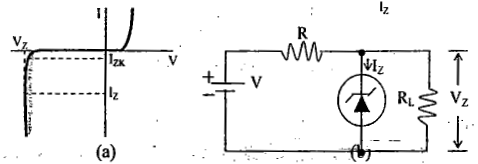
The reverse voltage characteristic of a semiconductor diode, including the breakdown region is shown in fig.7 (a). By reverse biasing, the diode is operating in the breakdown region as shown in fig.7 (b)
The diode will regulate the load voltage against variations in load current and against variations in supply voltage V because, in the break down region, large changes in diode current produce only small changes in diode voltage.
The upper limit on diode current is determined by the power dissipation rating of the diode. The thermally generated electrons and holes acquire sufficient energy from the applied potential to produce new carriers by removing valence electrons from their bonds. These new carriers, in turn, produce additional carriers again through the process of disrupting bonds. This cumulative process is referred to as "avalanche multiplication". It results in the flow of large reverse currents, and the diode finds itself in the region of "avalanche breakdown".
Even if the initially available carriers do not acquire sufficient energy to disrupt bonds, it is possible to initiate breakdown through a direct rupture of the bonds because of the existing of the strong electric field. Under these circumstances the break down is referred to as the "Zener Breakdown". This Zener effect is now known to play with breakdown voltages below about 6V.
If the reference voltage is above 6V, where the physical mechanism involved is avalanche multiplication, the temperature coefficient is positive.
However, below 6V, where true Zener breakdown is involved, the temperature coefficient is negative.
The Zener breakdown voltage decreases with temperature. The value of the avalanche voltage must increase with increased temperature.
The capacitance across a breakdown diode is the transition capacitance. High power avalanche diodes have very large capacitances. Cr is from 10 to 10,000 pf are common.
 (a) The volt-ampere Characteristic of an avalanche, or Zener, diode.
(b) A circuit in which such a diode is used to regulate the voltage across RL against changes due to variations in load current and supply voltage.
Tunnel Diode
A p-n junction diode has an impurity concentration of about 1 part in 108. With this amount of doping, the width of the depletion layer, which constitutes a potential barrier at the junction, is of the order of 5 microns (5 x 10⁻⁶ m). If the concentration of impurity atoms is greatly increased, say, to 1 part in 103 (corresponding to a density in excess of 1019 /cm3), the device characteristics are completely changed. This new diode was announced in 1958 by Esaki.
Tunneling Phenomenon: The width of the junction barrier varies inversely as the square root of impurity concentration and therefore is reduced from 5 microns to less than 100A
(10-6 cm). This thickness is only about one-fifth the wavelength of visible light.
Classically, a particle must have energy at least equal to the height of a potential barrier if it is to move from one side of the barrier to the other. However, for barriers as thin as those estimated above in Esaki diode, the Schrodinger equation indicates that there is a large probability that an electron will penetrate through the barrier. This quantum mechanical behavior is referred to as "tunneling", and hence these high-impurity density p-n junction devices are called "tunnel diodes".
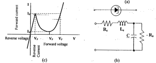
 (a) symbol for a tunnel diode (b) small-signal model of a tunnel diode in the negative resistance region (c) The volt-ampere characteristic of a tunnel diode.
Characteristics of a Tunnel Diode
The tunnel diode exhibits a negative resistance characteristic between the peak current Ip and the minimum value Iv, called the valley current. The tunnel diode useful in pulse and digital circuitry. The small-signal model for operation in negative resistance region is indicated in fig.8.(b)
Tunnel diode is used as very high speed switch. Switching times of the order of a - nanosecond are reasonable and times as low as 50 p sec have been obtained. A second application is as a high frequency (microwave) oscillator. The voltages Vv and VF have negative temperature coefficients of about 1.0 mV/0C:
Tunnel diode Applications:
- Tunnel diode is used as an ultra-high speed switch, switching speed of the order of ns or ps
- As logic memory storage device
- As microwave oscillator
- In relaxation oscillator circuit
- As an amplifier.
Advantages
- Low noise
- Ease of operation
- Highspeed
- Low power
Disadvantages
- Voltage range over which it can be operated is 1 V or less.
- Being a two terminal device, there is no isolation between the input and output circuit.
FAQs on Junction Theory & Different Types of Diodes & Their Characteristics - 2
| 1. What is the junction theory of diode resistance? |  |
| 2. What are the different types of diodes and their characteristics? |  |
| 3. How does a rectifier diode work? |  |
| 4. What is the purpose of a Zener diode? |  |
| 5. How are light-emitting diodes (LEDs) different from regular diodes? |  |
 | Explore Courses for Electronics and Communication Engineering (ECE) exam |  |
 | Get EduRev Notes directly in your Google search |  |


