P-N Junction Diode | Solid State Physics, Devices & Electronics PDF Download
P-N Junction Diode
Semiconductor Diode
In an n-type material the electron is called the majority carrier and the hole the minority carrier. In an p-type material the holes are the majority carrier and the electrons are minority carrier.
If the two materials are “joined” the electrons and holes in the region of the junction will combine resulting in a lack of carriers in the region near the junction. This region of uncovered positive and negative ions is called the depletion region due to the depletion of mobile carriers in this region.
Since the diode is two terminal devices, the application of a voltage across its terminals leaves three possibilities: no bias (VD = 0V ) , forward bias (VD > 0V ) and reverse bias (VD<0V). Each is a condition that will result in a response that one must clearly understand if the device is to be applied effectively.
➤ No Applied Bias
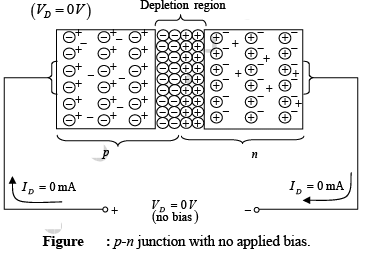 Under no bias condition, any minority carriers (holes) in the n-type material that find themselves within the depletion region will pass directly into the p-type material. The closer the minority carrier is to the junction, the greater the attraction for the layer of negative ions and the less the opposition of the positive ions in the depletion region of the n-type material. For further discussions we shall assume that all the minority carriers in the n-type material that find themselves in the depletion region due to their random motion will pass directly into the p-type material. Similar discussion can be applied to the minority carriers (electrons) of the p-type material.
The majority carriers (electrons) of the n-type material must overcome the attractive forces of the layer of positive ions in the n-type material and the shield of negative ions in the p-type material in order to migrate into the area beyond the depletion region of the p-type material. Again the same type of discussion can be applied to the majority carriers (holes) of the p-type material.
In the absence of an applied bias voltage, the net flow of charge in any one direction for a semiconductor diode is zero.
➤ Reverse Bias Condition
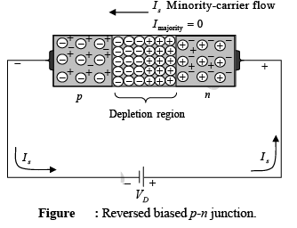
If an external potential of V volts is applied across the p-n junction such that the positive terminal is connected to the n-type material and the negative terminal is connected to the p-type material, the number of uncovered positive ions in the depletion region of the n-type material will increase due to the large number of “free” electrons drawn to the positive potential of the applied voltage.
For similar reasons, the number of uncovered negative ions will increase in the p-type material. The net effect, therefore, is a widening of the depletion region. This widening of the depletion region will establish too great a barrier for the majority carriers to overcome, effectively reducing the majority carrier flow to zero.
The number of minority carriers, however, that find themselves entering the depletion region will not change, resulting in minority-carrier flow. The current that exists under reverse bias conditions is called the reverse saturation current and is represented by
Is or I0.
Forward Bias Condition (VD > 0V)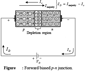
A forward-bias or “on” condition is established by applying the positive potential to the p-type material and the negative potential to the n-type material as shown in figure. Thus a semiconductor diode is forward-biased when the association p-type positive and n-type negative has been established.
The application of a forward-bias potential VD will “pressure” electrons in the n-type material and holes in the p-type material to recombine with the ions near the boundary and reduce the width of the depletion region. The resulting minority-carrier flow of electrons from the p-type material to the n-type material (and of holes from the n-type material to the p-type material) has not changed in magnitude (since the conduction level is controlled primarily by the limited number of impurities in the material), but the reduction in the width of the depletion region has resulted in a heavy majority flow across the junction. An electron in the n-type material now “sees” a reduced barrier at the junction due to the reduced depletion region and a strong attraction for the positive potential applied to the p-type material. As the applied bias increases in magnitude the depletion region will continue to decrease in width until a flood of electrons can pass through the junction, resulting in an exponential rise in current as shown in the forward-bias region of the characteristics.
➤ Ideal Diode
Before examining the construction and characteristics of an actual device, we first consider the ideal device, to provide a basis for comparison. The ideal diode is a two-terminal device having the symbol and characteristics shown in figure 2.4(a) and 2.4(b), respectively.
Ideally, a diode will conduct current in the direction defined by the arrow in the symbol and act like an open circuit to any attempt to establish current in the opposite direction. In essence: The characteristics of an ideal diode are those of a switch that can conduct current in only one direction. 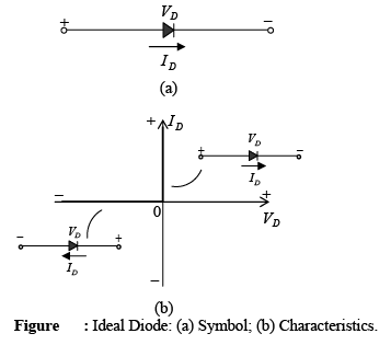
The ideal diode, therefore, is a short circuit in the region of conduction and is an open circuit in the region of non conduction.
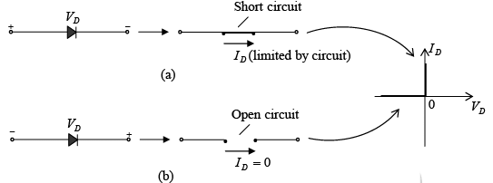
Figure : (a) Conduction and (b) non-conduction states of the ideal diode as determined by the applied bias.
➤ Diode Characteristics (Vγ = 0.7V for Si and Vγ =0.3V for Ge)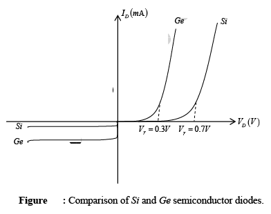
It is clear from the characteristics of figure that to forward bias the diode minimum voltage of Vγ is required. This voltage Vγ is called cut-in voltage of the diode. The closer the upward swing is to the vertical axis, the more “ideal” the device. However, the other characteristics of silicon as compared to germanium still make it the choice in the majority of commercially available units.
➤ Diode Equation
 where Is = reverse saturation current,
VT = kT/e is volt equivalent of temperature and η = 1 for Ge and η = 2 for Si devices.
Note: The reverse saturation current in a germanium diode is normally larger by a factor of about 1000 than the reverse saturation current in a silicon diode of comparable ratings.
Is is in the range of μA for a Ge diode and nA for a silicon diode at room temperature.
➤ Breakdown Diodes
Diodes which are designed with adequate power-dissipation capabilities to operate in the breakdown region may be employed as voltage-reference or constant-voltage devices. Such diodes are known as avalanche, breakdown or Zener diodes. They are used characteristically in the manner indicated in the figure.
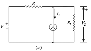
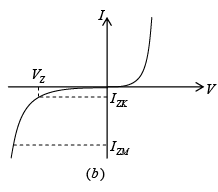 Figure: (a) Zener diode as voltage regulator (b) Zener charachteristics.
The source V and resistor R are selected so that initially, the diode is operating in the breakdown region. Here the diode voltage, which is also the voltage across the load RL, is VZ, and the diode current is IZ. The diode will now regulate the load voltage against variations in load current and against variations in supply V, because in the break-down region only small changes in diode voltage produce large changes in diode current. Moreover, as load current or supply voltage changes, the diode current will accommodate itself to these changes to maintain a nearly constant load voltage. The diode will continue to regulate until the circuit operation requires the diode current to fall to IZK, in the neighborhood of the knee of the diode volt-ampere curve. The upper limit on diode current is determined by the power dissipation rating of the diode.
➤ The Temperature Dependence of the V-I Characteristics
The volt-ampere relationship contains the temperature implicitly in the two symbols VT and Is. If the temperature is increased at a fixed voltage, the current increases. However if we now reduce V, then I may be brought back to its previous value. It is found that for either silicon or germanium (at room temperature)  in order to maintain a constant value of I. It should be noted that
  decreases with increasing T.
Diode Resistances
➤ DC or Static Resistance
The application of a dc voltage to a circuit containing a semiconductor diode will result in an operating point on the characteristic curve that will not change with time. The resistance of the diode at the operating point can be found simply by finding the corresponding levels of VD and ID as shown in figure and applying the following equation:
RD = VD/ID
The dc resistance levels at the knee and below will be greater than the resistance levels obtained for the vertical rise section of the characteristics. The resistance levels in the reverse-bias region will naturally be quite high. Since ohmmeters typically employ a relatively constant current source, the resistance determined will be at a preset current level (typically, a few milliamperes).
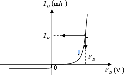
Figure : Determining the dc resistance of a diode at a particular operating point.
➤ AC or Dynamic Resistance
The dc resistance of a diode is independent of the shape of the characteristic in the region surrounding the point of interest. If a sinusoidal rather than dc input is applied, the situation will change completely. The varying input will move the instantaneous operating point up and down a region of the characteristics and thus defines a specific change in current and voltage as shown in figure (a). With no applied varying signal, the point of operation would be the Q-point appearing on figure determined by the applied dc levels. The designation Q-point is derived from the word quiescent which means “still or unvarying.”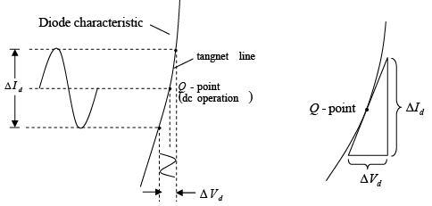
Figure : (a) Defining ac Resistance. (b) Determining the ac Resistance at a Q-point.
A straight line drawn tangent to the curve through the Q-point as shown in figure (b) will define a particular change in voltage and current that can be used to determine the ac or dynamic resistance for this region of the diode characteristics. An effort should be made to keep the change in voltage and current as small as possible and equidistant to either side of the Q-point. In equation form rd = ΔVd/ΔId where ∆ signifies a finite change in the quantity.
For small-signal operation the dynamic resistance r is an important parameter and is defined as the reciprocal of the slope of the volt ampere characteristic r = dV/dI
The dynamic resistance is not a constant, but depends upon the operating voltage.
For a semiconductor diode, the dynamic conductance g ≡ 1/r
At room temperature, for η = 1, r = 26/I, where I is in mA and r is in Ω. For a forward current of 26 mA the dynamic resistance is 1Ω.
Diode Capacitances
➤ Space-Charge or Transition Capacitance
A reverse bias causes majority carriers to move away from the junction, thereby uncovering more immobile charges. Hence the thickness of the space charge layer at the junction increases with reverse voltage. The increased in uncovered charge with applied voltage may be considered a capacitive effect. We may define an incremental capacitance CT by: CT = |dQ/dV| where dQ is the increase in charge caused by a change dV in voltage. It follows from this definition that a change in voltage dV in a time dt will result in a current i = dQ/dt given by i = CT(dV/dt) where CT is not a constant, but depends upon the magnitude of the reverse voltage.
➤ Diffusion Capacitance
For a forward bias a capacitance which is much larger than the transition capacitance lies in the injected charge stored near the junction outside the transition region. It is convenient to introduce an incremental capacitance, defined as the rate of change of injected charge with voltage, called the diffusion or storage, capacitance CD.
Charge control description of a diode
If the bias is in the forward direction, the potential barrier at the junction is lowered and holes from the p-side enter the n- side. Similarly electrons from the n-side move into the p-side. This process of minority-carrier injection has been discussed earlier. The excess hole density falls off exponentially with distance.
Assume that one side of the diode, say the p material, is so heavily doped in comparison with the n side that the current I is carried across the junction entirely by holes moving from the p to the n side or I =Ipn (0). The excess minority charge Q will then exist only on the n side.
Now I = Q/τ, where τ = τp = mean life for holes.
The above equation states that the diode current (which consists of holes crossing the junction from the p to the n side) is proportional to the stored charge Q of excess minority carriers. The factor of proportionality is the reciprocal of the decay time constant (the mean lifetimeτ) of the minority carriers. Thus in the steady state, the current I supplies minority carriers at the rate at which these carriers are disappearing because of the process of recombination.
Static Derivation of CD
Since, I = Q/τ and 
where g = dI/dV is the diode incremental conductance and r = 1/g is the diode incremental resistance.
Thus 
We see that the diffusion capacitance is proportional to the current I. In the above derivation we have assumed that the diode current I is due to holes only. If this assumption is not satisfied then above equation gives the diffusion capacitance  due
due
holes only and a similar expression can be obtained for the diffusion capacitance  due
due
to electrons. The total diffusion capacitance can then be obtained as the sum of  and
and 
Note: For a reverse bias, g is very small and CD may be neglected compared with CT. For a forward current, on the other hand, CD is usually much larger than CT.
Despite the large value of CD, the time constant rCD may not be excessive because the dynamic forward resistance r = 1/g is small. Thus rCD = τ. Hence, the diode time constant equals the mean lifetime of minority carriers, which lies in the range of nanoseconds (ns) to hundreds of microseconds(μs).
Load Line Analysis
The applied load will normally have an important impact on the point or region of operation of a device. If the analysis is performed in a graphical manner, a line can be drawn on the characteristics of the device that represents the applied load. The intersection of the load line with the characteristics will determine the point of operation of the system. Such an analysis is, for obvious reasons, called load-line analysis.
Consider the network of figure 2.10(a) employing a diode having the characteristics of figure (b). Note in figure (a) that the “pressure” established by the battery is to establish a current through the series circuit in the clockwise direction. The fact that this current and the defined direction of conduction of the diode are a “match” reveals that the diode is in the “on” state and conduction has been established. The resulting polarity across the diode will be as shown in figure (a) and the first quadrant (VD and ID positive) of figure (b) will be the region of interest – the forward-bias region.
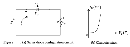
Applying Kirchhoff’s voltage law to the series circuit of figure (a) will result in
-E + VD + VR = 0 ⇒ E = VD + VR
⇒ E = VD + IDR
The two variables of above equation (VD and ID) are the same as the diode axis variables of figure (a). This similarity permits a plotting of the equation on the same characteristics of figure (b).
The intersections of the load line on the characteristics can easily be determined if one simply employs the fact that anywhere on the horizontal axis ID = 0A and anywhere on the vertical axis VD = 0 V. 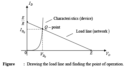
If we set VD = 0V in equation E = VD + IDR and solve for ID, we have the magnitude of
ID on the vertical axis. Thus E =VD+ IDR = 0V + IDR and 
If we set ID = 0A in equation E = VD + IDR and solve for VD, we have the magnitude of
VD on the horizontal axis. Thus E = VD + ( 0A) R and VD = 
A straight line drawn between the two points will define the load line as depicted in figure . Change the level of R (the load) and the intersection on the vertical axis will change. The result will be a change in the slope of the load line and a different point of intersection between the load line and the device characteristics.
We now have a load line defined by the network and a characteristics curve defined by the device. The point of intersection between the two is the point of operation for this circuit. By simply drawing a line down to the horizontal axis the diode voltage  can be determined, whereas a horizontal line from the point of intersection to the vertical axis will provide the level of
  . The current ID is actually the current through the entire series configuration of figure (a). The point of operation is usually called the quiescent point (abbreviated “Q-point”) to reflect its “still, unmoving” qualities as defined by a dc network.
The solution obtained at the intersection of the two curves is the same that would be obtained by a simultaneous mathematical solution of equations E = VD + IDR and 
Series Diode Configurations with DC Inputs
In this section the approximate model is utilized to investigate a number of series diode configurations with dc inputs. The procedure described can, in fact, be applied to networks with any number of diodes in a variety of configurations.
For each configuration the state of each diode must first be determined. Which diodes are “on” and which are “off”? Once determined, the appropriate equivalent can be substituted and the remaining parameters of the network determined.
In general, a diode is in the “on” state if the current established by the applied sources is such that its direction matches that of the arrow in the diode symbol, and VD ≥ 0.7 V for silicon and VD ≥ 0.3 V for germanium.
For each configuration, mentally replace the diodes with resistive elements and note the resulting direction as established by the applied voltages (“pressure”). If the resulting direction is a “match” with the arrow in the diode symbol, conduction above is, of course, contingent on the supply having a voltage greater than the “turn-on” voltage ( Vγ ) of each diode.
If a diode is in the “on” state, one can either place a 0.7 V drop across the element, or the network can be redrawn with the Vγ equivalent circuit. In time the preference will probably simply be to include the 0.7 V drop across each “on” diode and draw a line through each diode in the “off” or open state. Initially, however, the substitution method will be utilized to ensure that the proper voltage and current levels are determined.
The series circuit of figure (a) will be used to demonstrate the approach described in the paragraphs above. The state of the diode is first determined by mentally replacing the diode with a resistive element as shown in figure (b). The resulting direction of I is a match with the arrow in the diode symbol and since E > Vγ the diode is in the “on” state. The network is then redrawn as shown in figure (c) with the appropriate equivalent model for the forward-biased silicon diode. Note for future reference that the polarity of VD is the same as would result if in fact the diode were a resistive element.
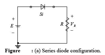
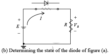

The resulting voltage and current levels are the following.
VD = Vγ, VR = E-Vγ and ID = IR = (VR/R).
In figure (a) the diode of figure (a) has been reversed. Mentally replacing the diode with a resistive element as shown in figure (b) will reveal that the resulting current direction does not match the arrow in the diode symbol. The diode is in the “off” state, resulting in the equivalent circuit of figure (c). Due to the open circuit, the diode current is 0 A and the voltage across the resistor R is the following:
VR = IRR = IDR = 0V
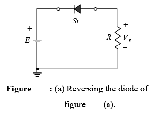
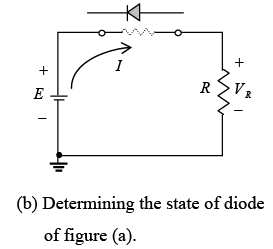
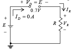 Figure (c): Substituting the equivalent model for the “off” diode of figure (a).
The fact that VR = 0V will establish E volts across the open circuit as defined by Kirchhoff’s voltage law. Always keep in mind that under any circumstances–dc, ac instantaneous values, pulses, and so on – Kirchhoff’s voltage law must be satisfied!
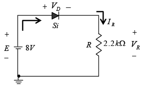
Example: For the series diode configuration of figure shown below, determine VD, VR, and ID.
Since the applied voltage establishes a current in the clockwise direction to match the arrow of the symbol and the diode is in the “on” state.
VD = 0.7 V, VR = E – VD = 8 V – 0.7 V = 7.3 V
Example: Repeat above example with the diode reversed.
Removing the diode, we find that the direction of I is opposite to the arrow in the diode symbol and the diode equivalent is the open circuit no matter which model is employed. The result is the network of figure shown below, where ID = 0 A due to the open circuit. Since VR = IRR, VR = (0)R = 0 V.
Applying Kirchhoff’s voltage law around the closed loop yields
-E +VD + VR = 0
and VD = E – VR = E – 0 = E = 8 V
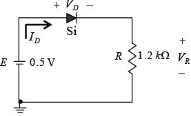
Example: For the series diode configuration of figure shown below, determine VD, VR, and ID.
Although the “pressure” establishes a current with the same direction as the arrow symbol the level of applied voltage is insufficient to turn the silicon diode “on”. The resulting voltage and current levels are therefore the following:
ID = 0 A, VR = IRR = IDR = (0 A) 1.2 kΩ = 0 V and VD = E = 0.5 V
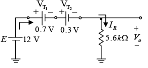
Example: Determine V0 and ID for the series circuit of figure shown below.
The resulting current has the same direction as the arrowheads of the symbols of both diodes, and the network of figure shown below results because E = 12V> ( 0.7 V + 0.3 V) = 1 V .Note the redrawn supply of 12 V and the polarity of V0 across the 5.6 kΩ resistor. The resulting voltage
Example: Determine I, V1, V2 and V0 for the series dc configuration of figure shown below.
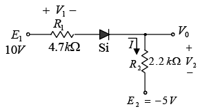
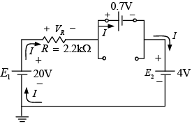
The sources are drawn and the current direction indicated as shown in figure below. Note that the “on” state is noted simply by the additional VD= 0.7 V on the figure. This eliminates the need to redraw the network and avoids any confusion that may result from the appearance of another source.
The resulting current through the circuit is,
and the voltages are V1 = IR1 = (2.07 mA) (4.7 kΩ) = 9.73 V
V2 = IR2 = (2.07 mA) (2.2 kΩ) = 4.55 V
Applying Kirchhoff’s voltage law to the output section in the clockwise direction will result in +E2 -V2 +V0 = 0 and V0 = V2 – E2 = 4.55 V – 5 V = - 0.45 V.
The minus sign indicates that V0 has a polarity opposite to that appearing in figure.
Parallel and Series–Parallel Configurations
The methods applied in series configurations can be extended to the analysis of parallel and series-parallel configurations. For each area of application, simply match the sequential series of steps applied to series diode configurations.
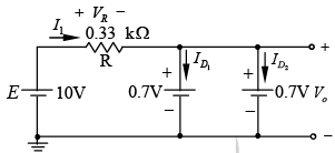
Example: Determine V0, I1, ID1 and ID2 for the parallel diode configuration as shown in figure. 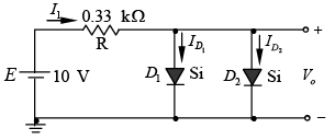
For the applied voltage the “pressure” of the source is to establish a current through each diode in the same direction as shown in figure below. Since the resulting current direction matches that of the arrow in each diode symbol and the applied voltage is greater than 0.7 V, both diodes are in the “on” state. The voltage across parallel elements is always the same and V0 = 0.7 V.
The currentAssuming diodes of similar characteristics,
Example: Determine the current I for the network shown in figure below.
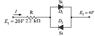
Redrawing the network as shown in figure reveals that the resulting current direction is such as to turn on diode D1 and turn off diode D2. The resulting current I is then
Rectifiers
➤ Half-Wave Rectification
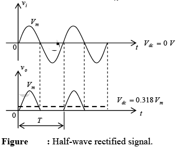
This circuit will generate a waveform vo that will have an average value of particular use in the ac-to-dc conversion process.
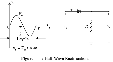
During the interval t = 0 → T/2 the polarity of the applied voltage is such as to establish “pressure” in the direction indicated and turn on the diode with the polarity appearing above the diode. Substituting the short-circuit equivalence for the ideal diode will result in the equivalent circuit shown in figure, where it is fairly obvious that the output signal is an exact replica of the applied signal. The two terminals defining the output voltage are connected directly to the applied signal via the short-circuit equivalence of the diode.

For the period t = T/2 → T, the polarity of input vi is shown in figure and the resulting polarity across the ideal diode produces an “off” state with an open circuit equivalent. The result is the absence of a path for charge to flow and v0 = 0V for the period T/2 → T . 
The process of removing one-half the input signal to establish a dc level is aptly called half-wave rectification.
The input vi and the output v0 were sketched together in figure for comparison purposes. The output signal v0 now has a net positive area above the axis over a full period and an average value determined by 
The process of removing one-half the input signal to establish a dc level is aptly called half-wave rectification.
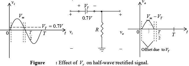
NOTE: The effect of using a silicon diode with Vγ = 0.7V is demonstrated in figure for the forward-bias region. The applied signal must now be at least 0.7V before the diode can turn “on.” For levels of vi less than 0.7V the diode is still in an open-circuit state and vo = 0V . When conducting, the difference between vo and vi is a fixed level of Vγ = 0.7V and v0 =vi−Vγ . The net effect is a reduction in area above the axis, which naturally reduces the resulting dc voltage level. For situations where Vm >>Vγ equation given below can be applied to determine the average value with a relatively high level of accuracy. 
Peak Inverse Voltage (PIV) or Peak Reverse Voltage (PRV)
It is the voltage rating that must not be exceeded in the reverse-bias region. The required PIV rating for the half-wave rectifier can be determined from figure, which displays the reverse-biased diode with maximum applied voltage. Applying Kirchhoff’s voltage law, it is fairly obvious that the PIV rating of the diode must equal or exceed the peak value of the applied voltage. Therefore, PIV rating ≥ Vm
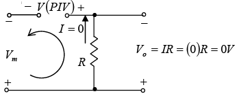
Figure : Determining the required PIV rating for the half-wave rectifier.
➤ Full Wave Rectification
(i) Bridge Network
The dc level obtained from a sinusoidal input can be improved 100% using a process called full-wave rectification. The most familiar network for performing such function appears in figure with its four diodes in a bridge configuration.
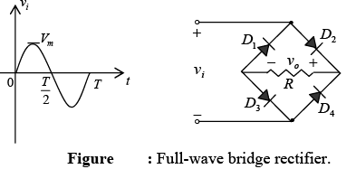
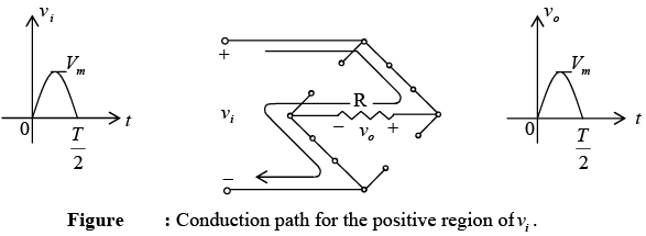
During period t = 0→T/2 the polarity of the input is shown in figure. The resulting polarities across the ideal diodes are shown to reveal that D2 and D3 are conducting while D1 and D4 are in the “off” state.

The net result is the configuration of figure, with its indicated current and polarity across R. Since the diodes are ideal the load voltage v0 =vi .
For the negative region of the input the conducting diodes are D1 and D4 , resulting in the configuration of figure. The important result is that the polarity across the load resistor R is the same as during positive half cycle. 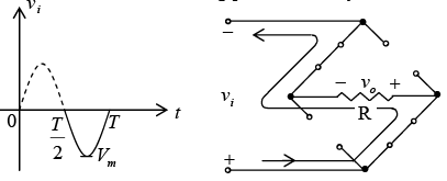
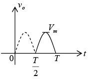
Figure : Conduction path for the negative region of vi.
Over one full cycle the input and output voltages will appear as shown in figure.
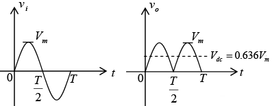
Figure : Input and output waveforms for a full-wave rectifier.
Since the area above the axis for one full cycle is now twice that obtained for half-wave system, the dc level has also been doubled and 
NOTE: If silicon rather than ideal diodes are employed as shown in figure, an application of Kirchhoff’s voltage law around the conduction path would result in
− vi + Vγ + vo + Vγ = 0 And vo = vi − 2Vγ
The peak value of the output voltage v0 is therefore 
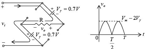
Figure : Determining Vomax for silicon diodes in the bridge configuration.
For situations where Vm >> 2Vγ equation given below can be applied to determine the average value with a relatively high level of accuracy.
Vdc ≌ 0.636(Vm − 2Vγ)
PIV
The required PIV of each diode (ideal) can be determined from figure obtained at the peak of the positive region of the input signal. For the indicated loop the maximum voltage across R is Vm and the PIV rating is defined by PIV ≥ Vm
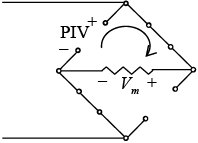
Figure : Determining the required PIV rating for the bridge configurations.
(ii) Center-Tapped transformer
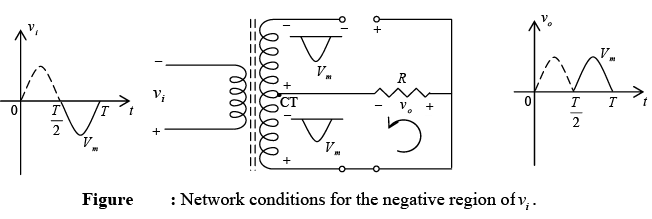
A second popular full-wave rectifier appears in figure with only two diodes but requiring a center-tapped (CT) transformer to establish the input signals across each section of the secondary of the transformer.
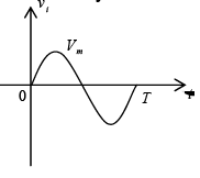
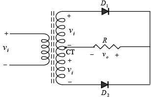
Figure : Centre-tapped transformer full-wave rectifier.
During the positive portion of vi applied to the primary of the transformer, the network will appear as shown in figure. D1 assumes the short-circuit equivalent and D2 the open circuit equivalent as detrmined by the secondary voltages and the resulting current directions. The output voltage v0 appears as shown in figure.

During the negative portion of the input the network appears as shown in figure, reversing the roles of the diodes but maintaining the same polarity for the voltage across the load resistor R. The net effect is the same output as that appearing in positive half cycle with the same dc levels.
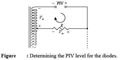
PIV : The network of figure will help us determine the net PIV for each diode for this full-wave rectifier. Inserting the maximum voltage for the secondary voltage and Vm as established by the adjoining loop will result in
PIV = Vsecondary + VR = Vm + Vm and PIV ≥ 2Vm .
Clippers
There are a variety of diode networks called clippers that have the ability to “clip” off a portion of the input signal without distorting the remaining part of the alternating waveform. The half-wave rectifier is an example of the simplest form of diode clipper– one resistor and diode. Depending on the orientation of the diode, the positive or negative region of the input signal is “clipped” off.
➤ Series Clippers (Positive and Negative)
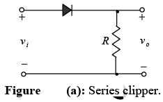
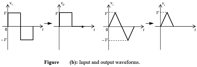
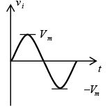
The response of the series configuration of figure (a) to a variety of alternating waveforms is provided in figure (b). Although first introduced as a half-wave rectifier (for sinusoidal waveforms), there are no boundaries on the type of signals that can be applied to a clipper.
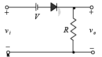
The addition of dc supply such as shown in figure can have a pronounced effect on the output of a clipper. Our initial discussion will be limited to ideal diodes and the effect of Vγ will be discussed later.
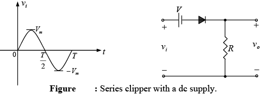
There is no general procedure for analyzing above networks, but there are a few thoughts to keep in mind before analyzing these circuits.
- Make a mental sketch of the response of the network based on the direction of the diode and the applied voltage levels.
The direction of the diode suggests that the signal vi must be positive to turn it on. The dc supply further requires that the voltage vi be greater than V volts to turn the diode on. The negative region of the input signal is “pressuring” the diode into the “off” state, supported further by the dc supply. In general, therefore, we can be quite sure that the diode is an open circuit (“off” state) for the negative region of the input signal.
- Determine the applied voltage (transition voltage) that will cause change in state for the diode.
For the ideal diode the transition between states will occur at the point on the characteristic where vd = 0V and id = 0A. Applying the condition id = 0A at vd = 0 will result in the configuration of figure, where it is recognized that the level of vi that will cause a transition in state is: vi =V.
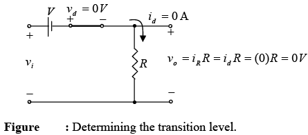
For an input voltage greater than V volts the diode is in the short-circuit state, while for input voltage less than V volts it is in the open-circuit or “off” state.
- Be continually aware of the defined terminals and polarity of vo.
When the diode is in the short-circuit state such as shown in figure, the output voltage vo can be determined by applying Kirchhoff’s voltage law in the clockwise direction.
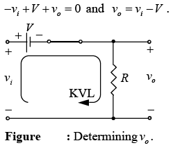
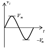
- It can be helpful to sketch the input signal above the output and determine the output at instantaneous values of the input.
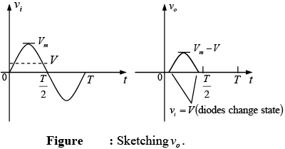
It is then possible that the output voltage can be sketched from the resulting data points of vo as demonstrated in figure.
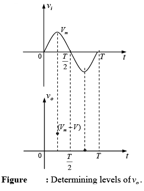
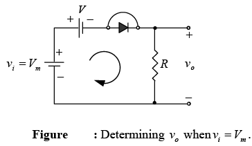
Keep in mind that at an instantaneous value of vi the input can be treated as a dc supply of that value and the corresponding dc value (the instantaneous value) of the output determined. For instance, at vi=Vm the network to be analyzed appears in figure.
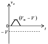
For Vm >V the diode is in the short-circuit state and vo =Vm − V . At vi =V the diodes change state and at vi =−Vm , vo = 0V and the complete curve for vo can be sketched as shown in figure.
Example: Determine the output waveform for the network shown in figure below.
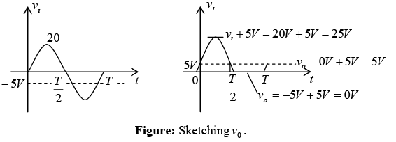
The diode will be in “on” state for the positive region of vi , especially when we note the aiding effect of V= 5V. The network will then appear as shown in figure (a) and v0 = vi + 5V. Substituting id = 0 at vd = 0 for the transition levels, we obtain the network of figure (b) and vi = -5V.
For vi more negative than − 5V the diode will enter its open-circuit state, while for voltages more positive than − 5V the diode is in the short-circuit state. The input and output voltage appear in figure shown below.
Example: Repeat above example for the square-wave input shown in figure below.
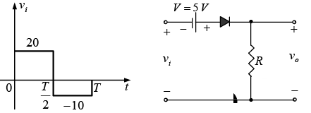
For vi = 20V(0→T/2) the network of figure (a) will result. The diode is in the short-circuit state and v0 = 20V+5V = 25V. For vi = -10V the network of figure (b) will result, placing the diode in the “off” state and v0 = iRR = 0 x R = 0V. The resulting output voltage appears in figure (c).
➤ Parallel Clippers (Positive and Negative)
The network of figure is the simplest of parallel diode configurations with the output for the same inputs. The analysis of parallel configurations is very similar to that applied to series configurations, as demonstrated in the next example.
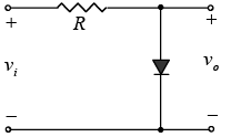
 Example: Determine v0 for the network of figure shown below.
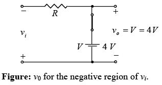
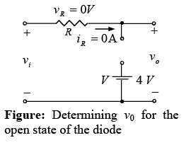
The polarity of the dc supply and the direction of the diode strongly suggest that the diode will be in the “on” state for the negative region of the input signal. For this region the network will appear as shown in figure below where the defined terminals for v0 require that v0 = V = 4V.
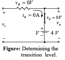
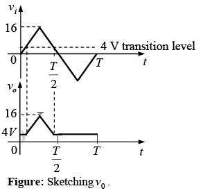
The transition state can be determined from figure shown below, where the condition id = 0A at vd = 0V has been imposed. The result is vi (transition) = V = 4V.
Since the dc supply is obviously “pressuring” the diode to stay in the short-circuit state, the input voltage must be greater than 4 V for the diode to be in the “off” state. Any input voltage less than 4V will result in a short-circuited diode.
For the open-circuit state the network will appear as shown in figure below, where v0 = vi. Completing the sketch of v0 results in the waveform of figure shown below.
To examine the effect of Vγ on the output voltage, the next example will specify a silicon diode rather than an ideal diode equivalent.
Example: Repeat above example using a silicon diode with Vγ = 0.7 V.
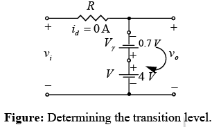
The transition voltage can first be determined by applying the condition id = 0 A at vd = 0.7V and obtaining the network of figure shown below. Applying Kirchhoff’s voltage law around the output loop in the clockwise direction, we find that − vi − Vγ + V = 0
and vi = V - Vγ = 4 - 0.7 = 3.3V
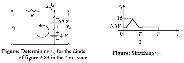
vR = idR = 0 x R = 0VFor input voltages greater than 3.3V, the diode will be an open circuit and v0 = vi . For input voltages of less than 3.3 V, the diode will be in the “on” state and the network of figure shown below results, where v0 = 3.3V.
Note that the only effect of Vγ was to drop the transition level to 3.3 V from 4 V.
There is no question that including the effects of Vγ was to drop the transition level to 3.3 V from 4V.
➤ Summary Clippers Networks
A variety of series and parallel clippers with the resulting output for the sinusoidal input are provided in figures shown below. In particular, note the response of the last configuration, with its ability to clip off a positive and a negative section as determined by the magnitude of the dc supplies.
➤ Simple Series Clippers (Ideal Diodes)
Positive:
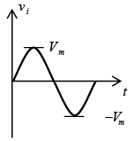
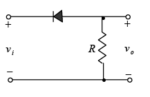
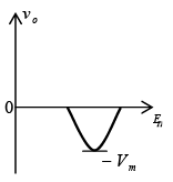
Negative:
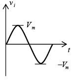
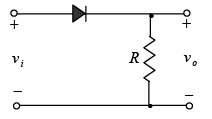
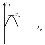
➤ Biased Series Clippers (Ideal Diodes)
Positive:
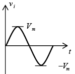
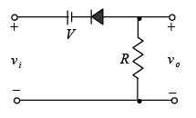
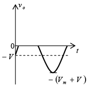
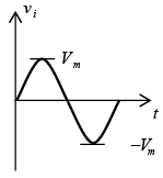
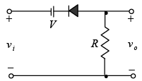
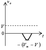
Negative
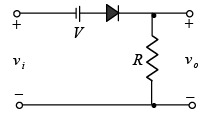
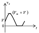
➤ Simple Parallel Clippers (Ideal Diodes)
Positive:
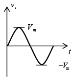
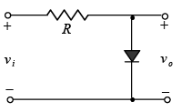
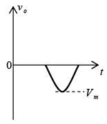
Negative:
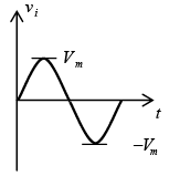
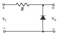
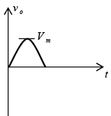
➤ Biased Parallel Clippers (Ideal Diodes)
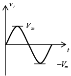
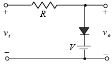
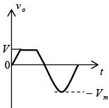
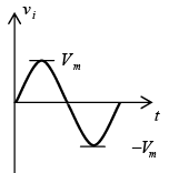
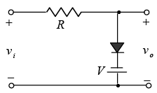
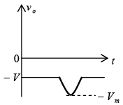
Negative:
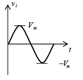
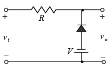
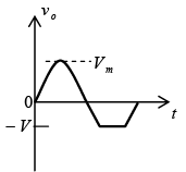
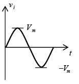
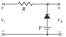
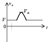
Miscellaneous
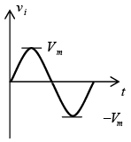
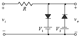
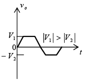
Clampers
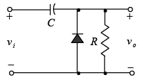
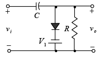
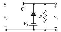
The clamping network is one that will “clamp” a signal to a different dc level. The network must have a capacitor, a diode, and a resistive element, but it can also employ an independent dc supply to introduce an additional shift. The magnitude of R and C must be chosen such that the time constant τ = RC is large enough to ensure that the voltage across the capacitor does not discharge significantly during the interval the diode is non-conducting. Throughout the analysis we will assume that for all practical purposes the capacitor will fully charge or discharge in five time constants.
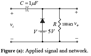
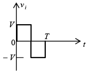
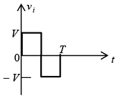
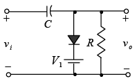
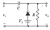
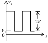
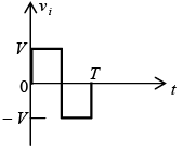
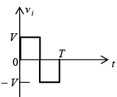
The network of figure will clamp the input signal to the zero level (for ideal diodes).
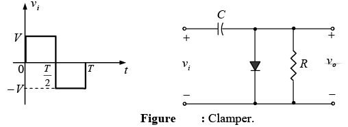
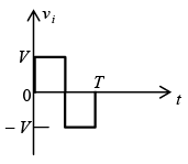
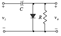
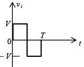
During the interval 0→T/2 the network will appear as shown in figure, with the diode in the “on” state effectively “shorting out” the effect of resistor R. The resulting RC time constant is so small (R is determined by the inherent resistance of the network) that the capacitor will charge to V volts very quickly. 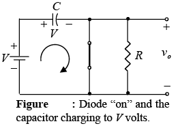
During this interval the output voltage is directly across the short circuit and vo = 0 V.
When the input switches to –V state, the network will appear as shown in figure 2.41, with the open-circuit equivalent for the diode determined by the applied signal and stored voltage across the capacitor-both “pressuring” current through the diode from cathode to anode.
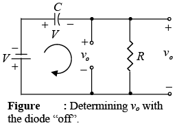
Now that R is back in the network the time constant determined by the RC product is sufficiently large to establish a discharge period 5τ much greater than the period T/2→T and it can be assumed on an approximate basis that the capacitor holds onto all its charge and therefore voltage (since V = Q/C) during this period.
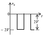
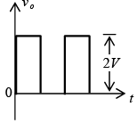
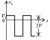
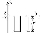
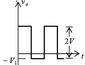
Applying Kirchhoff’s voltage law around the input loop will result in + V+ V+ vo = 0 and vo = – 2V.
The negative sign resulting from the fact that the polarity of 2V is opposite to the polarity defined for vo. The resulting output waveform appears in figure with the input signal. The output signal is clamped to 0 V for the interval 0 to T/2 but maintains the same total swing (2V) as the input.
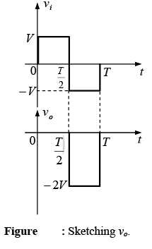
For a clamping network:
The total swing of the output is equal to the total swing of the input signal.
This fact is an excellent checking tool for the result obtained.
In general, the following steps may be helpful when analyzing clamping networks:
- Start the analysis of clamping networks by considering that part of the input signal that will forward bias the diode.
- During the period that the diode is in the “on” state, assume that the capacitor will charge up instantaneously to a voltage level determined by the network.
- Assume that during the period when the diode is in the “off” state the capacitor will hold on to its established voltage level.
- Throughout the analysis maintain a continual awareness of the location and reference polarity for vo to ensure that the proper levels for vo are obtained.
- Keep in mind the general rule that the total swing of the total output must match the swing of the input signal.
Example: Determine vo for the network of figure (a) for the input indicated.
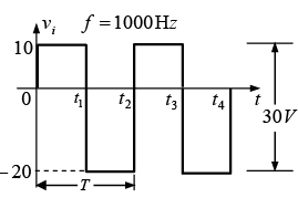
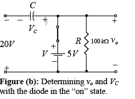
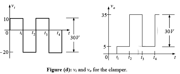
Note that the frequency is 1000 Hz, resulting in a period of 1 ms and an interval of 0.5 ms between levels. The analysis will begin with the period t1→ t2 of the input signal since the diode is in it short-circuit state as recommended by comment 1.
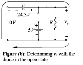
For this interval the network will appear as shown in figure (b). The output is across R, but it is also directly across the 5V battery if you follow the direct connection between the defined terminals for vo and the battery terminals. The result is vo = 5V for this interval.
Applying Kirchhoff’s voltage law around the input loop will result in +20V-VC +5V = 0 and VC = 25 V.
The capacitor will therefore, charge up to 25V, as stated in comment 2. In this case the resistor R is not shorted out by the diode but a Thevenin’s equivalent circuit of that portion of the network which includes the battery and the resistor will result in RTh = 0 Ω with ETh = V = 5 V.
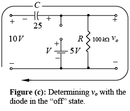
For the period t2 → t3 the network will appear as shown in figure (c). The open-circuit equivalent for the diode will remove the 5V battery from having any effect on vo, and applying Kirchhoff’s voltage law around the outside loop of the network will result in
-10 V - 25 V – vo = 0 and vo = 35 V.The time constant of the discharging network of figure (c) is determined by the product RC and has the magnitude: τ = RC = (100 kΩ) (0.1 μF) = 0.01 s = 10 ms
The total discharge time is therefore 5τ = 5 (10 ms) = 50 ms.
Since the interval t2 → t3 will only last for 0.5 ms, it certainly a good approximation that the capacitor will hold its voltage during the discharge period between pulses of the input signals. The resulting output appears in figure (d) with the input signal. Note that the output swing of 30 V matches the input swing as noted in step 5.
Example: Repeat above example using a silicon diode with Vγ = 0.7 V.
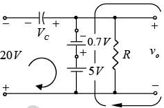
For the short-circuit state the network now takes form of figure (a) and vo can be determined by Kirchhoff’s voltage law in the output section.
Figure (a): Determining vo and VC with the diode in the “on” state-5V+0.7 V+ vo = 0
and vo = 5V – 0.7 V = 4.3 VFor the input section Kirchhoff’s voltage law will result in
+20V-VC –0.7V+5V = 0
and VC = 25 V – 0.7 V = 24.3 V.
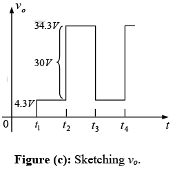
For the period t2 → t3 the network will now appear as in figure (b) with the only change being the voltage across the capacitor. Applying Kirchhoff’s voltage law yields
-10V-24.3 V+ vo = 0 and vo = 34.3 V.
The resulting output appears in figure (c) verifying the statements that the input and output swings are the same.
➤ Summary Clamping Networks
Zener Diode
The analysis of networks employing Zener diodes is quite similar to that applied to the analysis of semiconductor diodes. First the state of the diode must be determined followed by a substitution of the appropriate model and a determination of the other unknown quantities of the network. The Zener model to be employed for the “on” state and for the “off” state as defined by a voltage less than VZ but greater than 0V with the polarity indicated as shown in figure.
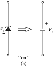
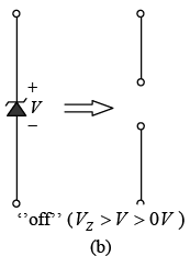
Figure : Zener diode equivalents for the (a) “on” and (b) “off” states.
➤ Case-I (Vi and RL fixed)
The simplest of Zener diode networks appears as shown in figure.
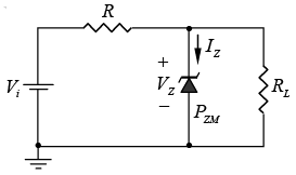 Figure: Basic Zener regulator.
The applied dc voltage is fixed, as is the load resistor. The analysis can fundamentally be broken down into two steps.
1. Determine the state of the Zener diode by removing it from the network and calculating the voltage across the resulting open circuit.
Open circuit voltage 
If V ≥VZ , the Zener is “on” and if V <VZ , the Zener is “off.”
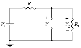
Figure : Determining the state of the Zener diode.
2. Substitute the appropriate equivalent circuit and solve for the desired unknowns.
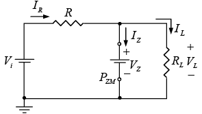
Figure : Substituting the Zener equivalent for the “on” situation.
When the Zener is “on” then VL =VZ and IR = IZ + IL ⇒ IZ = IR − IL
where 
Power dissipated by the Zener diode PZ =VZ IZ ≤ PZM .
Note: If the Zener diode is in the “on” state, the voltage across the diode is not V volts. When the system is turned on the Zener diode will turn “on” as soon as the voltage across the Zener diode is volts VZ . It will then “lock in” at this level and never reach the higher
level of V volts.
Zener diodes are most frequently used in regulator network or a reference voltage. A simple regulator designed to maintain a fixed voltage across the load RL . For values of applied voltage greater than required to turn the Zener diode “on,” the voltage across the load will be maintained at volts VZ. If the Zener diode is employed as a reference voltage, it will provide a level for comparison against other voltages.
Example: (a) For the Zener diode network of figure (a), determine VL ,VR, IZ and PZ. (b) Repeat part (a) with RL = 3 kΩ .
(a) Following the suggested procedure the network is redrawn as shown in figure (b).
Open circuit voltage

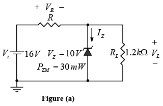
Since V = 8.73V is less than VZ = 10V the diode is in the “off” state. Substituting the open-circuit equivalent we will find that
VL =V= 8.73 V
VR =Vi− VL = 16 V − 8.73 V = 7.27 V
IZ = 0A and PZ =VZ IZ= 0 W .
(b) Open circuit voltage 
Since V = 12V is greater than VZ = 10V , the diode is in the “on” state and the network of figure (c) will result. 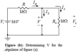
VL =VZ= 10 V and VR =Vi− VL = 6 V
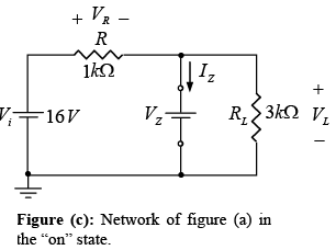
with 
and 
IZ = IR−IL = 6 mA −3.33 mA = 2.67 mA . The power dissipated, PZ =VZ IZ= 26.7 mW which is less than the specified 30 PZM =mW .
➤ Case-II ( fixed Vi and variable RL)
Due to the offset voltage VZ , there is a specific range of resistor values (and therefore load current) which will ensure that the Zener is in the “on” state. Too small a load resistance RL will result in a voltage VL across the load resistor less than VZ and the Zener device will be in the “off” state.
To determine the minimum load resistance that will turn the Zener diode on, simply calculate the value of RL that will result in a load voltage VL =VZ.
That is,  Solving for RL we have
Any load resistance value greater than the RL obtained from above equation will ensure that the Zener diode is in the “on” sate and the diode can be replaced by its VZ source equivalent.
This condition establishes the minimum RL , but in turn specifies the maximum IL as 
Once the diode is in the “on” state, the voltage across R remains fixed at VR = Vi-VZ and IR remains fixed at IR = VR/R
The Zener current IZ = IR−IL resulting in a minimum IZ when IL is a maximum and a maximum IZ when IL is a minimum value since IR is constant.
Since IZ is limited to IZM as provided on the data sheet, it does affect the range of RL and therefore IL. Substituting IZM for IZ establishes the minimum IL as  and the maximum load resistance as
Example: (a) For the network of figure shown determines the range of RL and IL that will result in RLV being maintained at 10 V.
(b) Determine the maximum voltage rating of the diode.
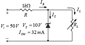
(a) To determine the value of RL that will turn the Zener diode on, apply equation
The voltage across the resistor R is then determined by equation
VR =Vi− VZ = 50 V − 10 V = 40 V and
The minimum level of IL is then determined by equation
with
➤ Case-III ( fixed RL and variable Vi)
For fixed values of RL , the voltage Vi must be sufficiently large to turn the Zener diode on. The minimum turn-on voltage  is determined by
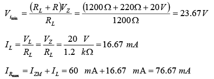
The maximum value of Vi is limited by the maximum Zener current IZM. Since IZM = IR−IL, 
Since IL is fixed at VZ /RL and IZM is the maximum value of IZ, the maximum Vi is defined by 
Example: Determine the range of values of Vi that will maintain the Zener diode in the “on” state.
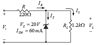
(76.67mA) (0.22 kΩ) + 20V =16.87V + 20V = 36.87V
➤ Zener as a Reference Levels
Two or more reference levels can be established by placing Zener diodes in series as shown in figure. As long as Vi is greater than the sum of  both diodes will be in the “on” state and the three reference voltages will be available.
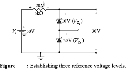
Two back-to-back Zener can also be used as an ac regulator as shown in figure. For the sinusoidal signal vi the circuit will appear as shown in figure at the instant vi = 10V. 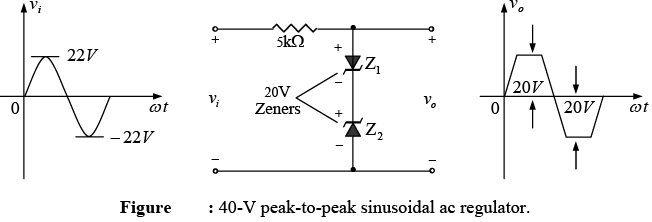
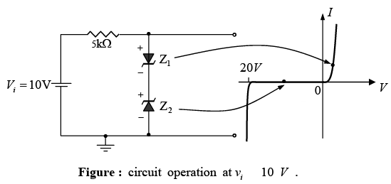
The region of operation for each diode is indicated in the adjoining figure. Note that Z1 is in a low-impedance region, while the impedance of Z2 is quite large, corresponding with the open-circuit representation. The result is that vo = vi when vi = 10V . The input and output will continue to duplicate each other until vi reaches 20 V. Z2 will then “turn on” (as a Zener diode) while Z1 will be in a region of conduction with a resistance level sufficiently small compared to the series 5 kΩ resistor to be considered a short circuit. The resulting output for the full range of vi is provided in figure. Note that the waveform is not purely sinusoidal, but its rms value is lower than that associated with a full 22 V peak signal.
|
91 videos|21 docs|25 tests
|
FAQs on P-N Junction Diode - Solid State Physics, Devices & Electronics
| 1. What is a P-N junction diode? |  |
| 2. How does a P-N junction diode work? |  |
| 3. What are the applications of P-N junction diodes? |  |
| 4. What is the forward and reverse bias of a P-N junction diode? |  |
| 5. What is the symbol and characteristics of a P-N junction diode? |  |

