Points to Remember: Solid State | Physical Chemistry PDF Download
Points to be Remembered
1. Classification of Solids : Solids are broadly classified into three categories - I. Crystalline, II. Amorphous and III. Pseudo solids.
- Crystalline Solids : Here, the constituents are arranged properly in a regular manner. Hence, these has a sharp melting point. It can sustain moderate external force. Example - NaCl, KCl etc.
- Amorphous Solids : Here, the constituents are not arranged in a regular way. Hence, these does not have any sharp melting point. It cannot sustain moderate external force. Example - CaCO3, MgCO3 etc.
- Pseudo Solids : These solids has properties in between crystalline and amorphous solids. Example - Pitch.
2. No. of Atoms Present in Different Lattices :
- No. of Atoms Present in Simple (Primitive) Cubic Lattice: In case of simple cubic lattice, there are eight corners. Each corner contains one atom. But, one atom at a corner is the equal part of such eight corners of such eight simple cubic lattices. Hence, the contribution of one atom in a particular simple cubic lattice is 1/8. As there are such eight comers present in a simple cubic lattice, total no. of atoms present in a simple cubic lattice : (8 X 1/8) = 1.
- No. of Atoms Present in Body Centred Cubic Lattice (B.C.C.): In case of bcc lattice, there are eight comers and each of which comer contains one atom. Hence, the total no. of atoms present at the comers is 1. But, one atom is present at the centre of the body centred cubic lattice. It is solely the part of the singly b.c.c lattice. Hence, the total contribution of atoms present in a b.c.c lattice are (1+1) = 2.
- No. of Atoms Present in Face Centred Cubic Lattice (F.C.C.): In case of bcc lattice, there are eight comers and each of which comer contains one atom. Hence, the total no. of atoms present at the comers is 1. Also, six atoms are present at the six faces of the f.c.c lattice. Each face is the common part of the two f.c.c lattice. Hence, contribution of one atom present in a face in each lattice is 1/2. Hence, the total no. of atoms present at the six faces are (6 x 1/2) =3. Hence, the total no. of atoms present in a f.c.c lattice are (1+3) =4.
3. Packing Fraction :
- Packing Fraction in Simple Cubic Lattice: The simple cubic lattice for a substance is shown below:
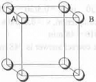
Let the edge length of the cube is a. Also, let the closest distance between the two atoms is d. Also, d = 2r
Hence, AB = BC = a = d = 2r
The no. of atoms present in simple cubic lattice is : 1.
Hence, volume occupied by the atoms = 4/3πr3..........(1)
The volume of the cube = a3 = 8r3
Hence, the packing fraction of the simple cubic lattice : (4 X πr3)/(24r3) = 0.52.
Hence, the packing fraction of a simple cubic lattice is : 0.52.
- Packing Fraction in Face Centred Cubic Lattice: The FCC lattice for a substance is shown below:
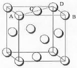 The total no. of atoms present in a FCC lattice = (1 + 3) = 4.
Let the edge length of the cube is a. Also, let the closest distance between the two atoms is d. Also, d = 2r
Hence, AB = BD = a and AD = 2AC = 2d = √[a2 + a2]
or, d = 2r = (√2)a√2 = a√2
or, r = a√2√2
or, a = 2√2r
Hence, volume occupied by the atoms = 4/3πr3 ............... ( 1 )
The volume of the cube = a3 = (2√2r)3
Hence, the packing fraction of the simple cubic lattice : ((16/3)πr3)/(16√2r3) = 0.74. - Packing Fraction in Body Centred Cubic Lattice: The BCC lattice for a substance is shown below:
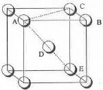 The total no. of atoms present in a BCC lattice = (1 + 1) = 2.Let the edge length of the cube is a. Also, let the closest distance between the two atoms is d. Also, d = 2r
Hence, AB = BC = CE = a and AC = √[a2 + a2] = a√2.
Hence, AE = √[2a2 + a2] or, 2d = 4r = a√3 or, a = 4r√3
Hence, volume occupied by the atoms = 4/3πr3................ (1)
The volume of the cube = a3 = (4r/√3)3
Hence, the packing fraction of the simple cubic lattice : {2.(4/3)πr3}/(4r/√3)3 = 0.68.
4. Crystal Defect: Crystal defect can be classified in the tabular form:
- Schottky Defect: It arises due to the missing of both cations and anions from their lattice sites. The missing of cations and anions will occur in such a way that the missing of total positive charge will become equal to the missing of total negative charge. Hence, in case of NaCl lattice if two Na+ ions are missing from their lattice sites then to maintain electrical neutrality two Cl- ions has to be missing. Similarly, in case of CaCl2 lattice if one Ca2+ ion is missing then to maintain electrical neutrality two CT has to be missing. It causes the decrease in density of the lattice. It mainly occurs in ionic lattices like NaCl, KCl etc.
- Frenkel Defect: It arises due to the occupancy o f ions (generally smaller size cations) at the interstitial positions instead of lattice sites. As no ions are missing, it does not cause any change in density. It mainly occurs in covalent lattices like AgBr, AgCl etc.
- Metal Excess: If one or, more anions are missing from a lattice then "such type of crystal defect will arise. Here, the electrical neutrality is maintained by occupying the interstitial positions by electrons. As here free electrons are available, on heating electronic transition to the higher level will occur resulting the generation of colour. ZnO is yellow on heating and white on cooling.
- Metal Deficiency: If one or, more cations are missing from their lattice sites then such type of crystal defect will occur. Here, the electrical neutrality is maintained by the oxidation of the adjacent metal. If one Fe2+ ion is missing from lattice site, the electrical neutrality will be maintained by oxidation of two Fe2+ ions into Fe3+ ions.
- Substitution by Impurity: Here, one or, more cations are missing. The electrical neutrality is maintained by adding external cation.
5. Semi-conductor: It can be of two types - n-type and p-type. These are described below:
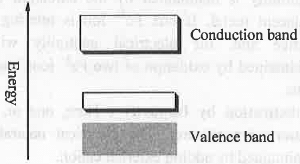
I. n-Type Semi-conductor: An n-type semi-conductor is formed when a small amount of penta valent (gr. V element) i.e. higher valent element like As is doped with tetra valent element like Si. Out of five, the four electrons of As will combine with the four electrons of the Si. The remaining one electron of As will form an negatively charge level which remain closer to the vacant conductance band. Hence, the forbidden energy gap that exist between valence and conductance band will decrease. Hence, less amount of energy will require to transfer electrons from newly formed electron dense level to conductance band causing semiconductivity. Hence, when Si is doped with a group V element, donor levels are created close to conduction band.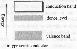 II. p-Type Semi-conductor: A p-type semi-conductor is formed when a small amount of tri-valent i.e. lower valent element like B is doped with tetra valent element like Si. The three electrons of B will combine with the three electrons of the Si. Hence, B will form a positively charge level which remain closer to the filled valence band. Hence, the forbidden energy gap that exist between valence and conductance band will decrease. Hence, less amount of energy will require to transfer electrons from filled valence band to the newly formed electron deficient conductance band causing semi-conductivity. Hence, the band structure given above represents a p-type semiconductor formed by doping Si with B.
|
90 videos|144 docs|67 tests
|
FAQs on Points to Remember: Solid State - Physical Chemistry
| 1. What is a solid state? |  |
| 2. What are the properties of a solid state? |  |
| 3. How are solids classified in the solid state? |  |
| 4. What is the difference between crystalline and amorphous solids in the solid state? |  |
| 5. How do solid-state materials conduct electricity? |  |


