Previous Year Questions- Operational Amplifiers - 2 | Analog and Digital Electronics - Electrical Engineering (EE) PDF Download
Q16: The operational amplifier shown in the figure is ideal. The input voltage (in Volt) is Vi = 2sin(2π × 2000t). The amplitude of the output voltage Vo (in Volt) is _______. (SET-2 (2015))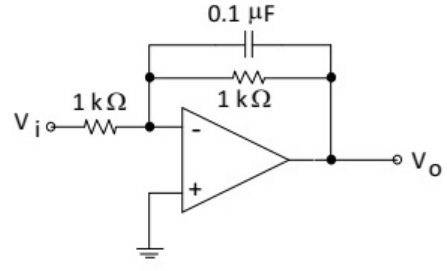
(a) 0.14
(b) 1.24
(c) 2.25
(d) 2.44
Ans: (b)
Sol: Vi = 2sin(2π × 2000t)
The transfer function of the system is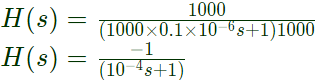 The input is 2sin(2π × 2000t)
ω = 4000π
V0 = 2∣H(jω)∣ω = 4000π × sin(4000πt − ϕ)
Output = 1.245sin(4000πt − 51.46°)
So, amplitude of output is 1.245.
Q17: The op-amp shown in the figure has a finite gain A = 1000 and an infinite input resistance. A step-voltage Vi = 1mV is applied at the input at time t = 0 as shown. Assuming that the operational amplifier is not saturated, the time constant (in millisecond) of the output voltage Vo is (SET-1 (2015))
(a) 1001
(b) 101
(c) 11
(d) 1
Ans: (a)
Sol: The circuit is Now, the gain of op-amp is 1000
So, Vo = 1000(V+ − V−)
Since V+ = 0 (grounded)
V- = VA
The above circuit can be redrawn as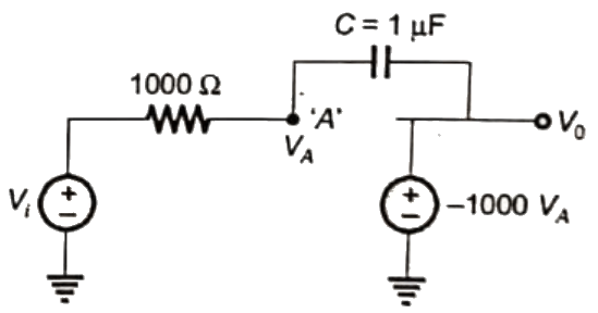 So, Vo = 1000VA
Now, KCL at node 'A' VA − Vi = (1001) × 1000VAsC
VA − Vi = s(1001000 × 10−6)VA
VA − s1.001VA = Vi Since, Vo = −1000VA
 Since, pole is at (1/1.001), so time constant is approax '1001'.
Q18: Consider the circuit shown in the figure. In this circuit R = 1kΩ, and C = 1μF. The input voltage is sinusoidal with a frequency of 50 Hz, represented as a phasor with magnitude Vi and phase angle 0 radian as shown in the figure. The output voltage is represented as a phasor with magnitude Vo and phase angle δ radian. What is the value of the output phase angle δ (in radian) relative to the phase angle of the input voltage? (SET-1 (2015))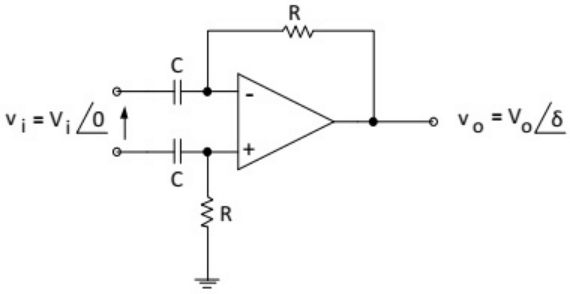 (a) 0
(a) 0
(b) π
(c) π/2
(d) −π/2
Ans: (d)
Sol: The circuit is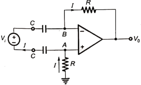 Since circuit has negative feedback, so with help of virtual short VA = VB
So, KVL in the loop from A to B given,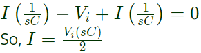 So, VA = −IR
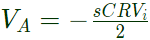 and VA = VB
So, 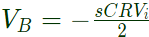
Now, 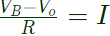
So, Vo = VB − IR
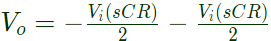 = −Vi(sCR)
So, Vo = −jωRCVi
So, Vo lag Vi by 90° or phase of Vo w.r.t Vi is −90°.
Q19: Of the four characteristics given below, which are the major requirements for an instrumentation amplifier?
P. High common mode rejection ratio
Q. High input impedance
R. High linearity
S. High output impedance (SET-1(2015))
(a) P, Q and R only
(b) P and R only
(c) P, Q and S only
(d) Q, R and S only
Ans: (a)
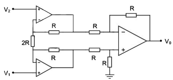
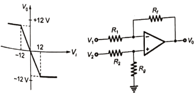
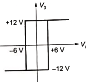
Q20: The transfer characteristic of the Op-amp circuit shown in figure is (SET-3(2014))
 (a)
(a) 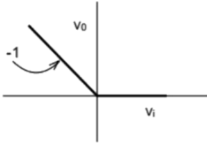 (b)
(b) 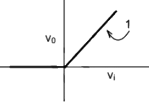 (c)
(c)  (d)
(d) 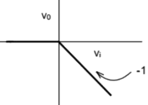 Ans: (c)
Sol: CASE-I: Vi > 0, the circuit will look like
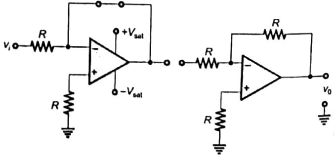 Hence Vo = 0
CASE-II: Vi < 0, the circuit will look like
 Vo = −V01 ...(iii)
From equation (ii) and (iii),
Vo = Vi
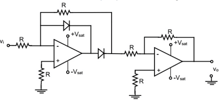
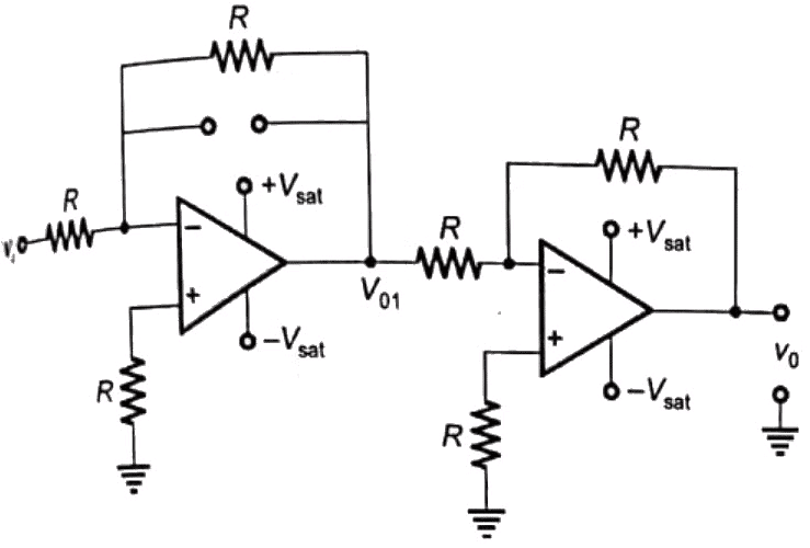
Q21: An operational amplifier circuit is shown in the figure.
 The output of the circuit for a given input vi is (SET-3 (2014))
(a)

(b) 
(c) 
(d) +Vsat or −Vsat
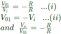
Sol: The circuit of op-amp '1' is a Schmitt trigger, therefore
V01 = ±Vsat
and the circuit of op-amp '2' is a non-inverting amplifier
 ⇒ V0 = 2V01
where, V01 = ±Vsat
Therefore, the answer is V0 = ±Vsat
Q22: A 10 kHz even-symmetric square ware is passed through a bandpass filter with centre frequency at 30 kHz and 3 dB passband of 6 kHz. The filter output is (SET-2 (2014))
(a) a highly attenuated square wave at 10 kHz
(b) nearly zero
(c) a nearly perfect cosine wave at 30 kHz
(d) a nearly perfect sine wave at 30 kHz
Ans: (c)
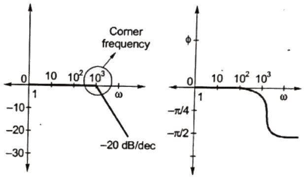
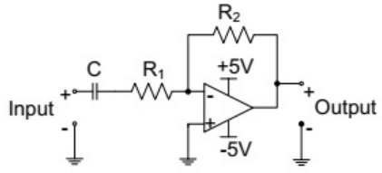
Q23: In the figure shown, assume the op-amp to be ideal. Which of the alternatives gives the correct Bode plote for the transfer function
 (SET-1 (2014))
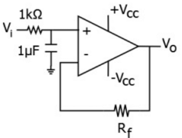 (a)
(a) 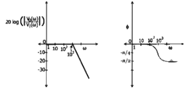 (b)
(b)  (c)
(c) 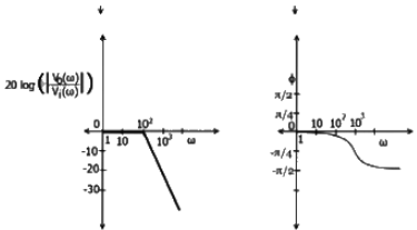 (d)
(d) 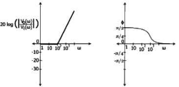 Ans: (a)
Sol:
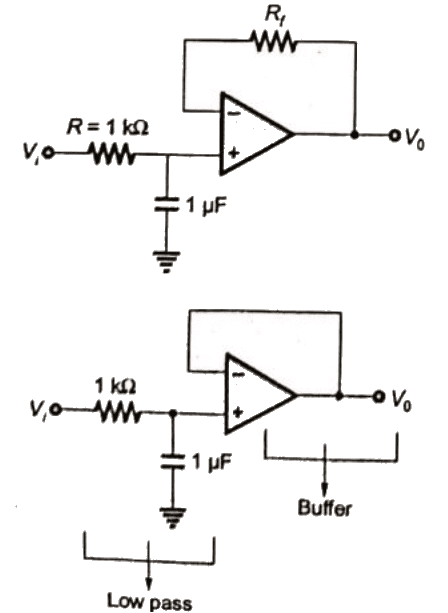 This filter is considered as low-pass filter (LPF). The transfer function for LPF
  ωc (corner frequency)= 103 rad/sec.
tha gain at low frequencies,
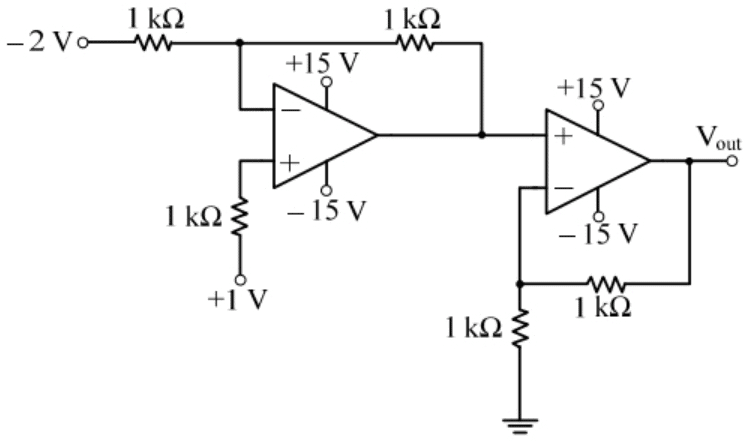
Q24: Given that the op-amps in the figure are ideal, the output voltage Vo is (SET-1 (2014))
 (a) (V1 − V2)
(b) 2(V1 − V2)
(c) (V1 − V2)/2
(d) (V1 + V2)
Ans: (b)
Sol: Op-amp '3' circuit is a differential amplifier so,
Vo = V01 − V02 ...(i)
Now, apply KCL at node '2'
 and apply KCL at node '1'
 From equation (i), (ii) and (iii), we get
V0 = 2(V1 − V2)
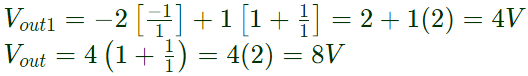
Q25: In the circuit shown below the op-amps are ideal. Then, Vout in Volts is (2013)
 (a) 4
(a) 4(b) 6
(c) 8
(d) 10
Ans: (c)
Sol: Output of the first op-amp
Q26: In the circuit shown below what is the output voltage (Vout) if a silicon transistor Q and an ideal op-amp are used? (2013)
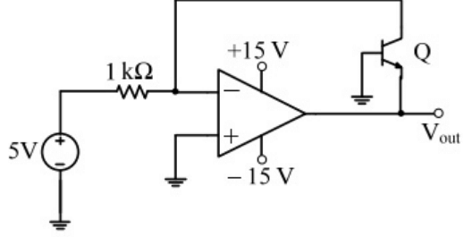 (a) -15 V
(b) -0.7V
(c) +0.7V
(d) +15V
Ans: (b)
Sol:
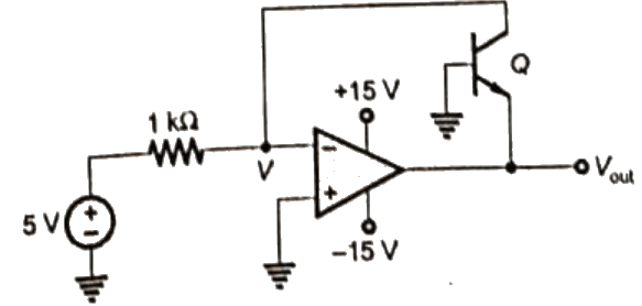 Using the concept of vitual ground, V = 0
 Vout = −0.7V
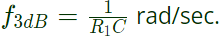
Q27: The circuit shown is a (2012)
 (a) low pass filter with f3dB =
(b) high pass filter with f3dB = 
(c) low pass filter with f3dB = 
(d) high pass filter with f3dB = 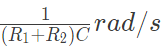
Ans: (b)
Sol: 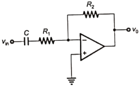
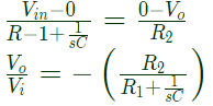 It is a high pass filter with
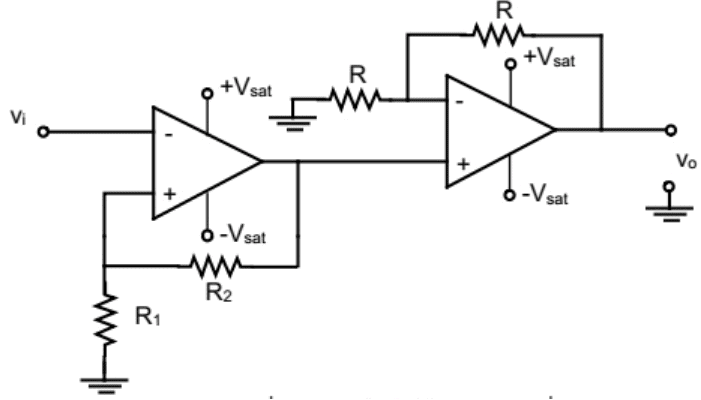
Q28: For the circuit shown below,
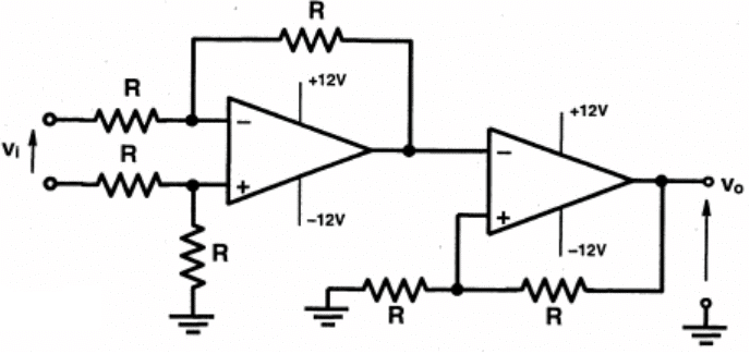 The CORRECT transfer characteristic is (2011)
(a)
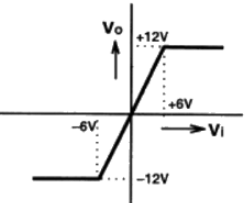 (b)
(b)  (c)
(c) 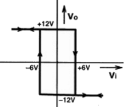 (d)
(d) 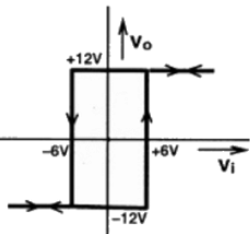 Ans: (d)
Sol: First section is differential amplifier having gain-1.
 Output is
 Second stage-schmitt trigger
Q29: A low-pass filter with a cut-off frequency of 30 Hz is cascaded with a high pass filter with a cut-off frequency of 20 Hz. The resultant system of filters will function as (2011)
(a) an all-pass filter
(b) an all-stop filter
(c) an band stop (band-reject) filter
(d) a band-pass filter
Ans: (d)
Sol:
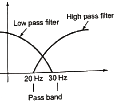 It is band pass filter.
Q30: Given that the op-amp is ideal, the output voltage V0 is (2010)
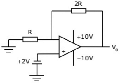 (a) 4V
(b) 6V
(c) 7.5V
(d) 12.12V
Ans: (b)
Sol:
 = (1 + 2)(2) = 6V
|
137 videos|143 docs|71 tests
|
FAQs on Previous Year Questions- Operational Amplifiers - 2 - Analog and Digital Electronics - Electrical Engineering (EE)

|
Dec 22, 2024 Last updated |

|
Explore Courses for Electrical Engineering (EE) exam
|
|
past year papers
,Previous Year Questions with Solutions
,Summary
,mock tests for examination
,MCQs
,Free
,Semester Notes
,Previous Year Questions- Operational Amplifiers - 2 | Analog and Digital Electronics - Electrical Engineering (EE)
,Extra Questions
,Viva Questions
,Objective type Questions
,Previous Year Questions- Operational Amplifiers - 2 | Analog and Digital Electronics - Electrical Engineering (EE)
,Important questions
,shortcuts and tricks
,Sample Paper
,Previous Year Questions- Operational Amplifiers - 2 | Analog and Digital Electronics - Electrical Engineering (EE)
,Exam
,ppt
,video lectures
,practice quizzes
,study material
;


Previous Year Questions- Operational Amplifiers - 2 Free PDF Download
Importance of Previous Year Questions- Operational Amplifiers - 2
Previous Year Questions- Operational Amplifiers - 2 Notes
Previous Year Questions- Operational Amplifiers - 2 Electrical Engineering (EE)
Study Previous Year Questions- Operational Amplifiers - 2 on the App
|
© EduRev
|
Education Revolution
|


|


