Physics Exam  >  Physics Notes  >  Solid State Physics, Devices & Electronics  >  Semiconductor Physics: Assignment

Semiconductor Physics: Assignment | Solid State Physics, Devices & Electronics PDF Download

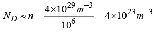
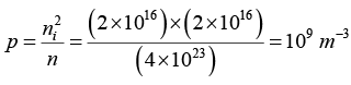
Q.1. Pure silicon at 300 K has equal electron and hole concentration of 2 x 10¹⁶ m-3.  It is doped by nitrogen to the extent one part in 106 silicon atom. If the density of silicon is 4 x 1029 m-3, then find the electron and hole concentration in the doped silicon.

Donor ion concentration Semiconductor Physics: Assignment | Solid State Physics, Devices & Electronics
According to Law of Mass Action, n.p = ni2
Semiconductor Physics: Assignment | Solid State Physics, Devices & Electronics

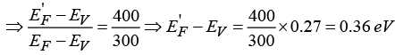
Q.2. In a p-type semiconductor, the Fermi level is 0.27 eV above the valance band at room temperature of 300 K . If the temperature is increased to 400 K , then find the new position of the Fermi-level. (Assume effective density of states to be independent of temperature).

EF-EV = kT ln NV/NA ⇒ 0.27 = 300k In NV/NA and E'F-EV = 400K In NV/NA

Semiconductor Physics: Assignment | Solid State Physics, Devices & Electronics

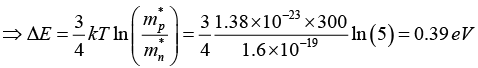
Q.3. The acceptor concentration in a sample of p -type silicon is increased by a factor of 50. Find the shift in the position of the Fermi level at 350K. 

EF-EV = kT ln (NV/NA)  and E'- EV = kT In (NV/50NA) = kT In (NV/NA) - kT In (50)
Thus shift is 

Semiconductor Physics: Assignment | Solid State Physics, Devices & Electronics
⇒ ΔE = 486 x 10-4 eV = 48.6 meV

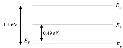
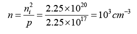
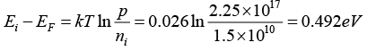
Q.4. A Si sample is doped with 2.25x10¹⁷ Al atoms/cm3 at 300 K. The intrinsic carrier concentration at 300 K is 1.5 x 1010 cm-3.
(a)What is the equilibrium electron and hole concentration at 300 K?
(b) Where is EF relative to Ei?

Since NA>>nwe can approximate nand p = 2.25 x 10 17Al

Semiconductor Physics: Assignment | Solid State Physics, Devices & Electronics

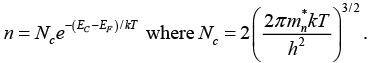
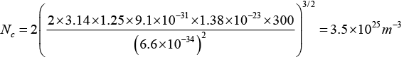
Q.5. For a given semiconductor the effective mass of the electron is 1.25me and the Fermi level is 0.3 eV below the conduction at 300 K . Determine the concentration of electrons in conduction band.

Semiconductor Physics: Assignment | Solid State Physics, Devices & Electronics
At 300 K, Semiconductor Physics: Assignment | Solid State Physics, Devices & Electronics
⇒ n = 3.5 x 1025 exp[-0.3x1.6x10-19 / 1.38x10-23x 300] = 32 x 1019m-3

Q.6. Consider an intrinsic semiconductor with energy band gap of 0.72 eV at 300 K . What will be shift in position of Fermi-level from the middle of the band gap if effective mass of hole is five times the effective mass of electrons?

Semiconductor Physics: Assignment | Solid State Physics, Devices & Electronics

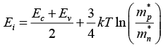
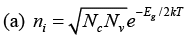
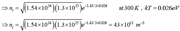
Q.7. Consider an intrinsic semiconductor with energy band gap of 1.43 eV , effective density of states in conduction band is 1.54 x 1024 m-3 and effective density of states in valance band is 1.3 x 1025 m-3 at 300 K.
(a) Determine the intrinsic carrier concentration of the semiconductor.
(b) Determine the effective masses of electrons and holes.

Semiconductor Physics: Assignment | Solid State Physics, Devices & Electronics

Semiconductor Physics: Assignment | Solid State Physics, Devices & Electronics
(b) At 300 K,
Semiconductor Physics: Assignment | Solid State Physics, Devices & Electronics 

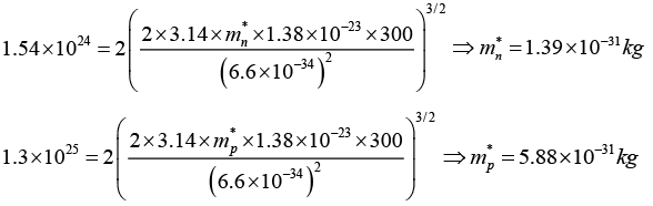
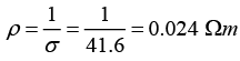
Q.8. A sample of Si has electron and hole mobilities of 0.13 and 0.05 m2V-1s-1 respectively at 300K.
(a) It is doped with P and Al with doping densities of 3.5 x 10²¹/m3 and 1.5 x 10²¹/m3 respectively. Find the resistivity of doped Si sample at 300K.
(b) It is doped with Ga and N with doping densities of 3.5 x 10²¹/m3 and 1.5 x 10²¹/m3 respectively. Find the conductivity of doped Si sample at 300 K.

(a) Resulting doped crystal is n-type and n= (3.5 - 1.5) x 1021/m3 = 2 x 10²¹/m3

σ = e(nnμ+ pnμp) ≈ ennμn = 1.6 x 10-19 x 2 x 1021 x 0.13 = 41.6Ω-1m-1
Semiconductor Physics: Assignment | Solid State Physics, Devices & Electronics
(b) Resulting doped crystal is p-type and pp = (3.5-1.5) x1021/m3 = 2 x 10²¹/m3
Semiconductor Physics: Assignment | Solid State Physics, Devices & Electronics 1.6 x 10-19 x 2 x 1021 x 0.05 = 16Ω-1m-1.

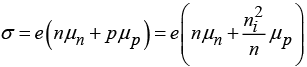
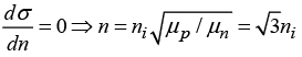
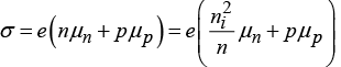
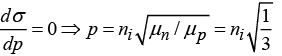
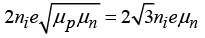
Q.9. Consider an extrinsic semiconductor with intrinsic concentration of ni. If μp and μn are mobility of holes and electron where μp = 3μn then
(a) Find the electron concentration at which semiconductor has minimum conductivity
(b) Find the hole concentration at which semiconductor have minimum conductivity
(c)  Find minimum conductivity σmin.

(a) Conductivity Semiconductor Physics: Assignment | Solid State Physics, Devices & Electronics
For minimum conductivity, Semiconductor Physics: Assignment | Solid State Physics, Devices & Electronics
(b) Conductivity Semiconductor Physics: Assignment | Solid State Physics, Devices & Electronics
For minimum conductivity, Semiconductor Physics: Assignment | Solid State Physics, Devices & Electronics
(c) Thus, σmin = Semiconductor Physics: Assignment | Solid State Physics, Devices & Electronics

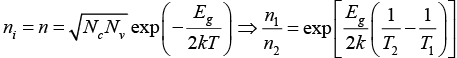
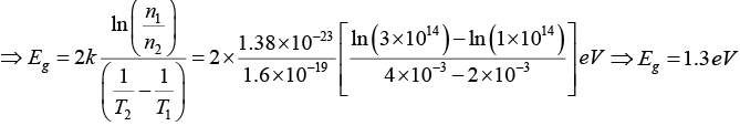
Q.10. In an intrinsic semiconductor, the free carrier concentration n (in cm-3) varies with temperature T (in Kelvin) as shown in the figure below.
If n1 = 3 x 10¹⁴m-3 and n2 = 1 x 10⁸m-3 and 1/T= 2 x 10⁻³K-1 and 1/T2= 4 x 10⁻³K-1.
Find the band gap energy of the semiconductor material. (Assume effective density of states and band gap energy to be independent of temperature).
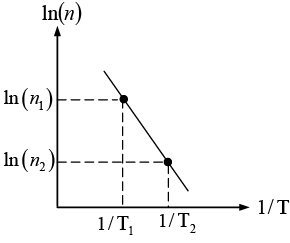
Semiconductor Physics: Assignment | Solid State Physics, Devices & Electronics

Since Semiconductor Physics: Assignment | Solid State Physics, Devices & Electronics
Semiconductor Physics: Assignment | Solid State Physics, Devices & Electronics

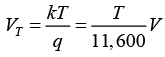
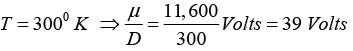
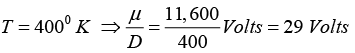
Q.11. Find the ratio of mobility (μ) and diffusion coefficient (D) for electrons in a semiconductor at temperature T = 270C and T = 1270C.

Semiconductor Physics: Assignment | Solid State Physics, Devices & Electronics where VT is the ‘Volt-equivalent of temperature’.
Semiconductor Physics: Assignment | Solid State Physics, Devices & Electronics
At temperature Semiconductor Physics: Assignment | Solid State Physics, Devices & Electronics

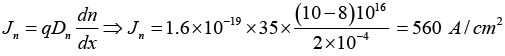
Q.12. The electron concentration in a sample of uniformly doped n-type silicon 300 K varies linearly from 1017/cm3 at x = 0 to 8x10¹⁶/cm3 at x = 2μm. Assume a situation that electrons are supplied to keep this concentration gradient constant with time. If electronics charge is 1.6 x 10⁻¹⁹ C and the diffusion constant Dn = 35cm2/s, find the current density in the silicon, if no electric field is present.

Semiconductor Physics: Assignment | Solid State Physics, Devices & Electronics 

Q.13. Determine the wavelength of light emitted from LED which is made up of GaAsP semiconductor whose forbidden energy gap is 1.875 eV. Mention the colour of the light emitted (Take h = 6.6 × 10⁻³⁴ Js).

E= hc / λ
Therefore
λ = h/ Eg  = 6.6 × 10−34 × 3 × 108  / 1.875 × 1.6 × 10−19 
= 660 nm
The wavelength 660 nm corresponds to red colour light.

Q.14. In a transistor connected in the common base configuration, α = 0.95 , IE = 1 mA . Calculate the values of IC and IB.

α = IC/IE
IC = α IE = 0.95 × 1 = 0.95 mA
IE = IB + IC 
∴ IB = IC − IE = 1 − 0.95 = 0.05 mA

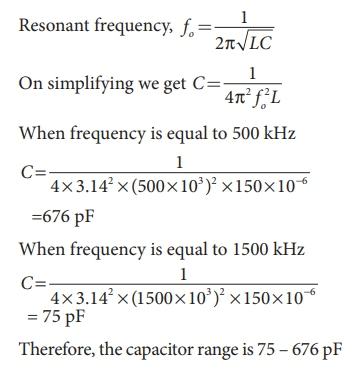
Q.15. Calculate the range of the variable capacitor that is to be used in a tuned-collector oscillator which has a fixed inductance of 150 μH. The frequency band is from 500 kHz to 1500 kHz.

Semiconductor Physics: Assignment | Solid State Physics, Devices & Electronics

Q.16. In the given figure of a voltage regulator, a Zener diode of breakdown voltage 15V is employed. Determine the current through the load resistance, the total current and the current through the diode. Use diode approximation.
Semiconductor Physics: Assignment | Solid State Physics, Devices & Electronics

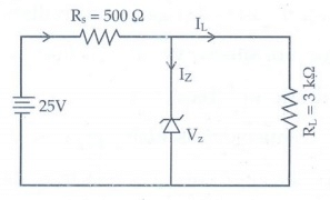
Voltage across RL(VO) = Vz = 15V
Voltage across RS(VRS) = 25 - 15 = 10V
current through RL is
IL = V0/RL = 15 / 3 × 103 = 5 × 10⁻³ A
IL = 5 mA
Current through RS is
I = VRS/RS = 10/500 = 20 × 10-3A
I = 20mA
Current through Zener diode is
IZ = I-IL = (20 - 5) × 10-3 Iz = 15mA

The document Semiconductor Physics: Assignment | Solid State Physics, Devices & Electronics is a part of the Physics Course Solid State Physics, Devices & Electronics.
All you need of Physics at this link: Physics
91 videos|21 docs|25 tests

FAQs on Semiconductor Physics: Assignment - Solid State Physics, Devices & Electronics

1. What is semiconductor physics?
Ans. Semiconductor physics is the branch of physics that deals with the behavior and properties of semiconductor materials. It involves the study of the electrical conductivity, energy band structure, carrier transport, and the interaction of light with semiconductors. This field is crucial for understanding the operation of semiconductor devices such as diodes, transistors, and integrated circuits.
2. How do semiconductors work?
Ans. Semiconductors work based on the concept of energy band theory. In a semiconductor, there are two energy bands: the valence band and the conduction band. The valence band contains the electrons that are tightly bound to their atoms, while the conduction band allows for the free movement of electrons. The energy gap between these two bands determines the conductivity of the semiconductor. When a semiconductor is subjected to an external electric field or light, electrons can be excited from the valence band to the conduction band, creating a flow of charge carriers. This process is known as carrier generation. By controlling the doping and biasing of the semiconductor material, one can control the flow of electrons and holes, enabling the functioning of various semiconductor devices.
3. What is doping in semiconductor physics?
Ans. Doping is the intentional introduction of impurities into a semiconductor material to alter its electrical conductivity. This process is essential for controlling the behavior of semiconductors and designing specific electronic devices. The two common types of doping are: - N-type doping: In this type, a small amount of impurity atoms, such as phosphorus or arsenic, which have more valence electrons than the semiconductor material, are added. These extra electrons become the majority charge carriers, increasing the conductivity of the semiconductor. - P-type doping: Here, impurity atoms, such as boron or gallium, with fewer valence electrons than the semiconductor material, are introduced. These impurities create "holes" or vacant spaces in the valence band, which act as majority charge carriers. The movement of these holes contributes to the conductivity of the semiconductor. By carefully controlling the doping process, it is possible to tailor the electrical properties of semiconductors for specific applications.
4. What are the primary applications of semiconductor physics?
Ans. Semiconductor physics has a wide range of applications in various fields. Some of the primary applications include: - Electronics: Semiconductor devices, such as diodes, transistors, and integrated circuits, form the backbone of modern electronics. These devices utilize the properties of semiconductors to control the flow of electrons and perform various functions in electronic circuits. - Optoelectronics: Semiconductors are used in optoelectronic devices, such as light-emitting diodes (LEDs), lasers, and photodetectors. These devices exploit the interaction of light with semiconductors to generate, control, and detect light signals. - Solar cells: Semiconductors play a crucial role in photovoltaic devices, commonly known as solar cells. These devices convert sunlight into electrical energy by utilizing the photoelectric effect in semiconductors. - Sensors: Many sensors, such as temperature sensors, pressure sensors, and gas sensors, are based on semiconductors. These sensors utilize the changes in electrical conductivity or other properties of semiconductors to detect and measure physical quantities. - Semiconductor lasers: Semiconductor lasers are widely used in various applications, including telecommunications, optical storage devices, and medical equipment. These lasers are based on the emission of light from semiconductors when electrically biased.
5. What are the challenges in semiconductor physics research?
Ans. Semiconductor physics research faces several challenges due to the complexity of semiconductor materials and devices. Some of the challenges include: - Miniaturization: As the demand for smaller and more efficient devices increases, researchers face the challenge of developing new materials and fabrication techniques to achieve the desired level of miniaturization. - Heat dissipation: With the shrinking size of semiconductor devices, heat dissipation becomes a significant challenge. Efficient thermal management strategies need to be developed to prevent overheating and ensure the reliable operation of devices. - Quantum effects: At the nanoscale, quantum effects become prominent in semiconductor physics. Understanding and controlling these effects is crucial for the development of quantum devices and technologies. - Material limitations: Existing semiconductor materials have certain limitations in terms of their performance and physical properties. Researchers are constantly exploring new materials with improved characteristics to overcome these limitations. - Energy efficiency: Semiconductor devices consume a significant amount of energy. Developing energy-efficient devices and exploring alternative energy sources for semiconductor applications is an ongoing challenge. Addressing these challenges requires continuous research and innovation in the field of semiconductor physics.
91 videos|21 docs|25 tests
Download as PDF
Explore Courses for Physics exam
Signup for Free!
Signup to see your scores go up within 7 days! Learn & Practice with 1000+ FREE Notes, Videos & Tests.
10M+ students study on EduRev
Related Searches

mock tests for examination

,

Important questions

,

past year papers

,

Free

,

Semiconductor Physics: Assignment | Solid State Physics

,

Devices & Electronics

,

ppt

,

video lectures

,

Objective type Questions

,

Extra Questions

,

pdf

,

Semester Notes

,

Semiconductor Physics: Assignment | Solid State Physics

,

practice quizzes

,

Previous Year Questions with Solutions

,

Summary

,

Sample Paper

,

Viva Questions

,

Exam

,

shortcuts and tricks

,

Devices & Electronics

,

MCQs

,

study material

,

Semiconductor Physics: Assignment | Solid State Physics

,

Devices & Electronics

;