Timers & Filters | Analog Circuits - Electronics and Communication Engineering (ECE) PDF Download
The 555 Timer Circuit
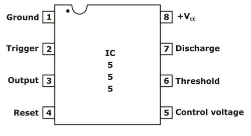 Pin diagram of 555 Timer
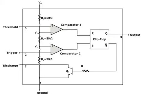 Block diagram representation of the internal circuit of the 555-IC timer
A block diagram representation of the 555-timer circuit is shown in figure . The circuit consist of two comparators, an SR flip-flop and a transistor Q1 that operates as a switch. One power supply VCC is required for operation. A resistive voltage divider, consisting of the three equal valued resistor R1 which is equal to 5kΩ is connected across VCC and establishes the reference or threshold voltages for the two comparators.
VTH = 2/3 VCC for comparator 1
And VTL = 2/3 VCC for comparator 2
SR flip-flop iworks as a bistable circuit having the complementary outputs, denoted as Q and
In set state, the output at Q is ‘high’ (approximately equal to VCC) and that at is ‘low’ (approximately equal to 0 V). In reset state, the output Q is low and
  is high.
The flipflop is set by applying a high level (VCC) to its set input terminal S and reset by applying to the reset input terminal R. The outputs of comparator 1 and comparator 2 respectively are connected to the set and reset input terminals of the flip flop.
The positive input terminal of the comparator 1 is connectecd to a external terminal of the 555 IC is labelled as Threshold. Similarly, the negative input terminal of comparator 2 is connected to an external terminal labelled as Trigger and the collector of transistor Q1 is connected to a terminal labelled discharge. finally, the output of flip flop Q is connected to output terminal.
Implementation of Monostable Multivibrator using 555 Timer
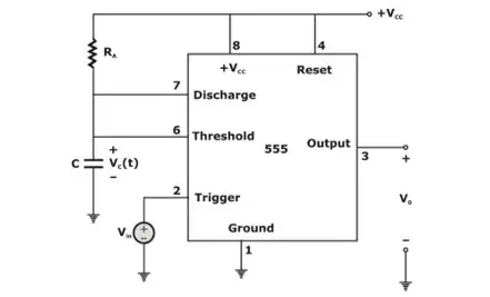 The 555 Circuit connected as Monostable Multivibrator
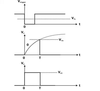 Wave form
The external circuitry and waveform of 555 IC as monostable multivibrator is shown in figure 2(a) & (b). Before applications of trigger pulse VT, The voltage at trigger input is high which is equal to +VCC. output and output voltage V0 is equal to 1. With  and output voltage V0 is equal to 1. When
  the discharging transistor Q1 undergoes to saturation and across the timing capacitor the voltage will be zero i.e., VC(t) = 0.
At t = 0, on the application of trigger VT (negative going pulse) <VCC/3 causes output of comparator C2 to be high i.e. S = 1. This will set the flip flop with This makes output voltage V0 = 0. Due to  the discharge transistor Q1 will get turned off. After the termination of trigger pulse, the flipflop will remain in state, since S = 0 and R = 0, So no change in state. The timing capacitor charges up exponentially toward final value of V+ through resistor R.
The capacitor voltage is given by
v(t) = V+(1 - et/RC) ......(i)
When v(t) = 2/3 V+, the threshold comparator output goes high, resetting the flip flop. Output then goes high and the output of the 555 goes low. The high output at
turns on the discharge transistor, allowing the timing capacitor to discharge to near zero volts. The circuit thus returns to its Quiescent state.
The width the output pulse is determined from equ. (i) by putting
v(t) = 2/3 v+ and t = T, then
(2/3)V+ = V+(1 - eT/RC)
solving for T,
The width of the output pulse is a function of only the external time constant RC, it is independent of supply voltage V+ and any internal circuit parameters.
Implementation of Astable Multivibrator using 555 Timer
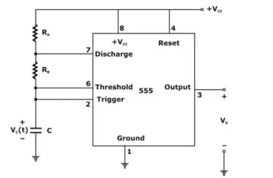 Astable Multivibrator 555 Circuit
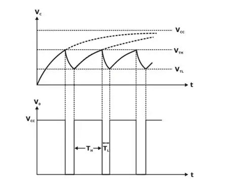 Waveform
In this the threshold and trigger input is connected together. In astable mode, the timing capacitor C charges through RA = RB until v(t) reaches 2/3 V+. The threshold comparator output then goes high, forcing the flip flop output to go high. The discharge transistor turns on, and the timing capacitor C discharges through RB and the discharge transistor.
The capacitor voltage decreases until it reaches (1/3)V+, at which point the trigger comparator switches stages and sends  low.
low.
The discharge transistor turns off, and the timing capacitor begins to recharge. When v(t) reaches the threshold level of (2/3) V+, the cycle repeat itself.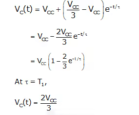
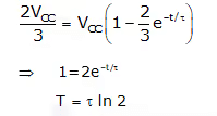
Therefore, charging time is given as
When the timing capacitor is discharging, during the time 0 < t’ < TD, the capacitor voltage is
Where τB = RBC, at t' = TD, the capacitor voltage reaches the trigger level and
solving equation (ii) for the timing capacitor discharge time TD, yields,
Total time to given as
T = TC + TD
The frequency of oscillation,

(i) Duty cycle: It is defined as the percentage of time the output is high during one period of oscillation. during the changing time TC, the output is high and during discharging time TD, the output is low.
Duty cycle of the circuit is always greater than 50%.
Active Filters
- An active filter means using amplifiers to improve the filter. An active filter generally uses an operational amplifier (op-amp) within its design.
- An electronic circuit that modifies the frequency spectrum of an arbitrary signal is called filter.
- A filter that modifies the spectrum producing amplification is said to be an active filter.
- Filtering components are resistance and capacitance only. Doesn’t include inductors
- Active components like op-amp, FET, transistors etc. are used
- It requires biasing voltage
- Its bandwidth is limited due to active component
- Gain is limited to the gain of active components used
- Small in size due to resistors and capacitors are used
- Due to active components like op-amp and FET input impedance is high
- Output impedance is low
- Basically used to suppress unwanted frequency components from information signals
- The main function of filters is to filter out required frequency components from mix frequency signal. They allow
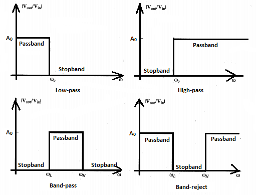
- They allow a range of frequency to pass that is known as pass band and rejects (or suppresses) other frequencies known as stop band.
- The cut-off frequency is the parameter that separates out these two bands. So depending upon these pass band and stop band there are four types of filters: Low pass filters, High pass filters, Band pass filters, and Band reject filters.

- An advantage of active filters:
- They can provide gain
- They can provide isolation because of the typical characteristic impedances of amplifiers
- They can be cascaded because of the typical characteristic impedances of amplifiers
- They can avoid the use of inductors greatly simplifying the design of the filters.
- Disadvantages of active filters:
- They are limited by the amplifier's bandwidth, and noise
- They need power supplies
- They dissipate more heat than a passive circuit.
Low Pass Filter (LPF)
- It allows to pass all the frequencies lower than its cut-off frequency and stops all other frequencies.
- A low-pass filter has a constant gain (=Vout/Vin) from 0 Hz to a high cut-off frequency fH.
- This cut off frequency is defined as the frequency where the voltage gain is reduced to 0.707, that is at fH the gain is down by 3 dB; after that (f > fH) it decreases as f increases.
- The frequencies between 0 Hz and fH are called pass band frequencies, whereas the frequencies beyond fH are the so-called stop band frequencies.
- A common use of a low-pass filter is to remove noise or other unwanted high-frequency components in a signal for which you are only interested in the dc or low-frequency components.
- Low-pass filters are also used to avoid aliasing in analog-digital conversion (which we will encounter in a few weeks). Correspondingly, a high-pass filter has a stop band for 0 < f < fL and where fL is the low cut off frequency.
- A simple, single-pole, low-pass filter (the integrator) is often used to stabilize amplifiers by rolling off the gain at higher frequencies where excessive phase shift may cause oscillations.
First Order Low Pass Filter Circuit: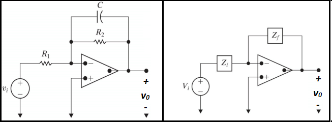
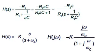
- The transfer function of the circuit:

- Gain:
K = R2/R1 - Cutoff Frequency:
ωc = 1/R2C
High pass filter (HPF)
- It allows to pass all the frequencies higher than its cut-off frequency and stops all other frequencies.
- A common use for a high-pass filter is to remove the dc component of a signal for which you are only interested in the ac components (such as an audio signal).
- A simple, single-pole, high-pass filter can be used to block dc offset in high gain amplifiers or single supply circuits.
- Filters can be used to separate signals, passing those of interest, and attenuating the unwanted frequencies.
First Order High Pass Filter Circuit:
- The transfer function of the circuit:


- Gain:
K = R2/R1
Cutoff Frequency:
ωc = 1/R1C
Band pass filter (BPF)
- It allows a passing band of frequencies between its higher cut-off and lower cut-off frequencies.
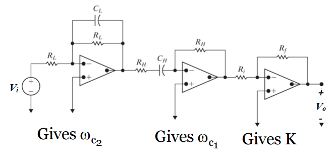
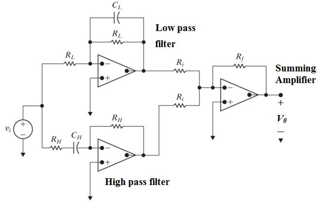
- If a high-pass filter and a low-pass filter are cascaded, a band pass filter is created.
- A bandpass filter has a pass band between two cut-off frequencies fH and fL, (fH > fL), and two stop bands 0 < f < fL and f > fH.
- The bandwidth of a bandpass filter is equal to fH -fL.
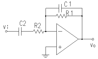
- The simplest band-pass filter can be made by combining the first order low pass and high pass filters.

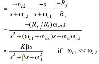
- This circuit will attenuate low frequencies (w<<1/R2C2) and high frequencies (w>>1/R1C1) but will pass intermediate frequencies with a gain of -R1/R2. However, this circuit cannot be used to make a filter with a very narrow band.

- First order band pass filter Circuit:

- Transfer function:


Band reject filter (BRF)
- It stops band of frequencies between its higher cut off and lower cut off frequencies.
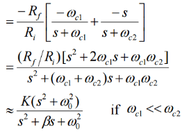
- A complement to the band pass filter is the band-reject or notch filter.
- The pass bands include frequencies below fL and above fH. The band from fL to fH is in the stop band.

- First order Band Stop filter Circuit:

- Transfer function:


Passive Filter
- A passive filter is made up entirely of passive components such as resistors, capacitors and inductors.
The difference between Active and Passive Filters
- Passive filters consume the energy of the signal, but no power gain is available; while active filters have a power gain.
- Active filters require an external power supply, while passive filters operate only on the signal input.
- Passive filters are constructed using only passive components (resistors, capacitors and inductors). Active filters may contain passive as well as active components.
- Active filters may contain passive as well as active components.
- Only passive filters use inductors. Active filters do not contain inductors.
- Only active filters use elements like op-amps and transistors, which are active elements.
- Theoretically, passive filters have no frequency limitations while active filters have limitations due to active elements.
- Passive filters can be used at high frequencies by using inductors.
- For Active filters, the frequency range is dependent on the bandwidth of the amplifier. Typically, to filter high-frequency signals, passive filters are used.
- Passive filters have a better stability and can withstand large currents.
- Passive filters are relatively cheaper than active filters.
|
3 videos|33 docs|64 tests
|
FAQs on Timers & Filters - Analog Circuits - Electronics and Communication Engineering (ECE)
| 1. What is a 555 timer circuit? |  |
| 2. How does a 555 timer circuit work? |  |
| 3. What are some common applications of a 555 timer circuit? |  |
| 4. Can a 555 timer circuit be used as an active filter? |  |
| 5. Are there any limitations or drawbacks of using a 555 timer circuit? |  |

|
Explore Courses for Electronics and Communication Engineering (ECE) exam
|

|
