Designing Asymmetric Logic Gates

Objectives
In this lecture you will learn the following
- Brief Introduction to Asymmetric Logic Gates
- Application of Asymmetric Logic Gates
- Analyzing Delays
- Pseudo NMOS Circuits
25.1 Brief Introduction to Asymmetric Logic Gates
Logic gates sometimes have different logical efforts for different inputs. We call such gates asymmetric. Asymmetric gates can speed up critical paths in a network by reducing the logical effort along the critical paths. This attractive property has a price, however the total logical effort of the logic gate increases. This lecture discusses design issues arising from biasing a gate to favor particular inputs.
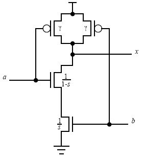
Fig 25.11: An asymmetric NAND gate
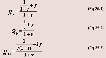
Fig 25.11 shows a NAND gate designed so that the widths of the two pull-down transistors can differ; input a has a width 1/(1-s), while input b has width 1/s. The parameter s, 0<s<1, called the symmetry factor, determines the amount by which the logic gate is asymmetric. If s=1/2, the gate is symmetric, the pull down transistors have equal sizes, and the logical effort is the same as calculated in the previous lectures. Values of s between 0 and 1/2 favor the a input by making its pull-down transistor smaller than the pull-down transistor for b. Values of s between 1/2 and 1 favor the b input.
The logical efforts per input for inputs a and b, and the logical effort  :
:
Choosing the least value possible for s, such as 0.01, minimizes the logical effort of input a. This design results in pull-down transistor of width 1.01 for input a and a transistor of width 100 for input b. The logical effort of input a is then  , or almost exactly 1. The logical effort of input b becomes
  , or about 34 if γ = 2. The total logical effort is about 35, again assuming γ = 2.
Extremely asymmetric designs, such as with s=0.1, are able to achieve a logical effort for one input that almost matches that of an inverter, namely 1. The price of this achievement is an enormous total logical effort, 35, as opposed to 8/3 for a symmetric design. Moreover, the huge size of the pull-down transistor will certainly cause layout problems, and the benefit of the reduced logical effort on input a may not be worth the enormous area of this transistor.
Less extreme asymmetry is more practical. If s=1/4, the pull-down transistors have widths 4/3 and 4, and the logical effort of input a is  , which is 1.1 if γ = 2. The logical effort of input b is 2, and the total logical effort is 3.1, which is very little more than 8/3, the total logical effort of the asymmetric design. This design achieves a logical effort for the favored input, a, that is only 10% greater than that of an inverter, without a huge increase in total logical effort.
25.2 Applications of Asymmetric Logic Gates
The principal application of asymmetric logic gates occurs when one path must be very fast. For example, in a ripple carry adder or counter, the carry path must be fast. The best design uses an asymmetric circuit that speeds the carry even though it retards the sum output.
Paradoxically, another important use of asymmetric logic gates occurs when a signal path may be unusually slow, as in a reset signal. Figure 25.21 shows a design for a buffer amplifier whose output is forced LOW, when the reset signal,  , is LOW. The buffer consists of two stages: a NAND gate and an inverter. During normal operation, when is HIGH, the first stage has an output drive equivalent to that of an inverter with pull-down width 6 and pull-up width 12, but the capacitive load on the in input is slightly larger than that of the corresponding inverter:
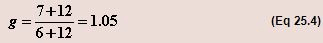
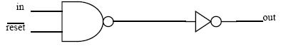
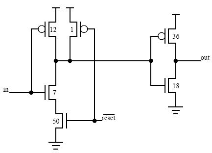
Fig 25.21: A buffer amplifier with a reset input. When is LOW, the output will always be LOW.
This circuit takes advantage of slow response allowed to changes on by using the smallest pull-up transistor possible. This choice reduces the area required to lay out the gate, partially compensating for the large area pull-down transistor. Area can be further reduced by sharing the the reset pull-down among multiple gates that switch at different times; this is known as Virtual Ground technique.
25.3 Analyzing Delays
We can model the delay of an individual stage of logic with one of the following two expressions:
 (Eq 25.5)
 (Eq 25.6)
where the delays are measured in terms of ζ. Notice that the logical efforts, parasitic delays, and stage delays differ for rising transitions (u) and falling transitions (d).
In path containing N logic gates, we use one of two equations for the path delays, depending on whether the final output of the path rises or falls. In the equations, i is the distance from the last stage, ranging from 0 for the final gate, to (N-1) for the first gate.
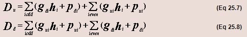
Equation 25.7 models the delay incurred when a network produces a rising output transition. In this equation, the first sum tallies the delay of falling transitions at the output of stages whose distance from the last stage is odd, and the second tallies the delay of the rising transitions at the output of stages whose distance from the last stage is even. Similarly Equation 25.8 models the falling output transition.
A reasonable goal is to minimize the average delay:
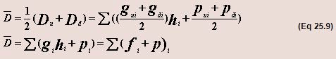
Then we have for the average delay:
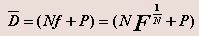 (Eq 25.10)
25.4 Pseudo NMOS Circuits
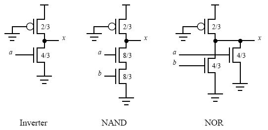
Fig 25.41 Pseudo-NMOS inverter, NAND and NOR gates, assuming μ = 2
The analysis presented in the previous delay analysis applies to pseudo-NMOS designs. The PMOS transistor produces 1/3rd of the current of the reference inverter, and the NMOS transistor stacks produce 4/3rd of the current of the reference inverter. For falling transitions, the output current is pull-down current minus the pull-up, i.e., 4/3 - 1/3 = 1. For rising transitions, the output current is just the pull-up current, 1/3.
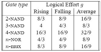
The inverter and NOR gate have an input capacitance of 4/3. The falling logical effort is the input capacitance divided by that of an inverter with the same output current, or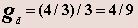 The rising logical effort is 3 times greater, gu = 4/3, because the current produced on a rising transition is only 1/3rd that of a falling transition. The average logical effort is g = (4/9+4/3)/2 = 8/9. This is independent of the number of inputs, explaining why pseudo-NMOS is a way to build fast, wide NOR gates.
Table 25.41 shows the rising, falling and average logical efforts of other pseudo-NMOS gates, assuming μ = 2 and a 4:1 pull-down to pull-up strength ratio.
FAQs on Designing Asymmetric Logic Gates
| 1. What are asymmetric logic gates? |  |
| 2. How do asymmetric logic gates differ from symmetric logic gates? | |
| 3. What are some examples of asymmetric logic gates? | |
| 4. How are asymmetric logic gates used in digital circuit design? | |
| 5. What are the advantages of using asymmetric logic gates? | |

