Power Dissipation in CMOS Circuits

Objectives
In this lecture you will learn the following
- Motivation
- Effect of Power Disipation
- How to Reduce Temperature
- Components of Power Disipation
- Static Power Dissipation
- Dynamic Power Dissipation
- Methods to Reduce Power Disipation
- Short-Circuit Power Dissipation
26.1 Motivation
Why is power dissipation so important? Power dissipation considerations have become important not only from reliability point of view, but they have assumed greater importance by the advent of portable battery driven devices like laptops, cell phones, PDAs etc.
26.2 Effects Of Power Dissipation
When power is dissipated, it invariably leads to rise in temperature of the chip. This rise in temperature affects the device both when the device is off as well as when the device is on.
When the device is off, it leads to increase in the number of intrinsic carriers, ni by the following relation:
 (Eq 26.1)
From this relation it can be seen that as temperature increases, it leads to increase in the number of intrinsic carriers in the semiconductor. The majority carriers, contributed by the impurity atoms, are less affected by increase in temperature. Hence the device becomes more intrinsic.
As temperature increases, leakage current, which directly depends on minority carrier concentration, increases which leads to further increase in temperature. Ultimately, the device might break down, if the increase in temperature is not taken care of by time to time removal of the dissipated heat
A ON device wont be affected much by minority carrier increase, but will be affected by  which decrease with increase in temperature and lead to change in ID. Hence the device performance might not meet the required specifications.
Also, power dissipation is more critical in battery powered applications as the greater power dissipated, the battery life will be.
26.3 How To Reduce Temperature
The heat generated due to power dissipation can be taken away by the use of heat sinks. A heat sink has lower thermal resistance than the package and hence draws heat from it. For the heat to be effectively removed, the rate of heat transfer from the area of heat generation to the ambient should be greater than the rate of heat generation. This rate of heat transfer depends on the thermal resistance.
The thermal resistance, θ is given by the following relation:
 (Eq 26.2)
where,
l = length,
A = Area and
σc = thermal conductivity of the heat sink
From the above relation it can be seen that large σc implies smaller θ .
θ is also given by the relation,
 (Eq 26.3)
Using this relation, we can see that for a given power dissipation, PD
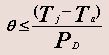 (Eq 26.4)
where,
 = junction temperature, and
 = ambient temperature.
Heat sink materials are generally coated black to radiate more energy
26.4 Components Of Power Dissipation
Unlike bipolar technologies, where a majority of power dissipation is static, the bulk of power dissipation in properly designed CMOS circuits is the dynamic charging and discharging of capacitances. Thus, a majority of the low power design methodology is dedicated to reducing this predominant factor of power dissipation.
There are three main sources of power dissipation:
- Static power dissipation (PS)
- Dynamic power dissipation (DS)
- Short circuit power dissipation (PSC)
Thus the total power dissipation, PD, is
 (Eq 26.5)
26.5 Static Power Dissipation
Consider the complementary CMOS gate, shown in Figure 26.51
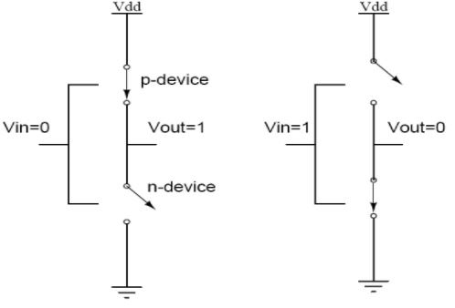
Fig 26.51: CMOS inverter model for static power dissipation evaluation
When input = '0', the associated n-device is off and the p-device is on. The output voltage is VDD or logic '1'. When the input = '1', the associated n-device is on and the p-device turns off. The output voltage is '0' volts or VSS. It can be seen that one of the transistors is always off when the gate is in either of these logic states. Since no current flows into the gate terminal, and there is no DC current path from VDD to VSS, the resultant quiescent (steady-state) current, and hence power Ps, is zero.
However, there is some small static dissipation due to reverse bias leakage between diffusion regions and the substrate. In addition, subthreshold conduction can contribute to the static dissipation. A simple model that describes the parasitic diodes for a CMOS inverter should be looked at in order to have an understanding of the leakage involved in the device. The source-drain diffusions and the n-well diffusion form parasitic diodes. In the model, a parasitic diode exists between n-well and the substrate. Since parasitic diodes are reverse biased, only their leakage current contributes to static power dissipation. The leakage current is described by the diode equation:
where, 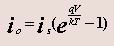 (Eq 26.6)
 = reverse saturation current
V = diode voltage
q = electronic charge
k = Boltzmann's constant
T = temperature
The static power dissipation is the product of the device leakage current and the supply voltage:
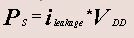 (Eq 26.7)
26.6 Dynamic Power Dissipation
During switching, either from '0' to '1' or, alternatively, from '1' to '0', both n- and p-transistors are on for a short period of time. This results in a short current pulse from VDD to VSS. Current is also required to charge and discharge the output capacitive load. This latter term is usually the dominant term. The current pulse from VDD to VSS results in a 'short-circuit'dissipation that is dependent on the input rise/fall time, the load capacitance and the gate design.
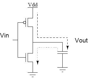
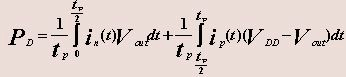
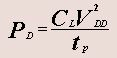
Fig 26.61: Power dissipation due to charging/discharging of capacitor
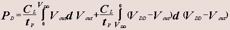
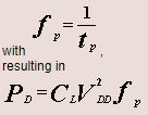
he dynamic dissipation can be modeled by assuming that the rise and fall time of the step input is much less than the repetition period. The average dynamic power, PD , dissipated during switching for a square-wave input, Vis, having a repetition frequency of  is given by
 (Eq 26.8)
where
in = n-device transient current
ip = p-device transient current
For a step input and with 
 (Eq 26.9)
 (Eq 26.10)
 (Eq 26.11)
Thus for a repetitive step input the average power that is dissipated is proportional to the energy required to charge and discharge the circuit capacitance. The important factor to be noted here is that Eq 26.11 shows power to be proportional to switching frequency but independent of device parameters.
The power dissipation also depends on the switching activity, denoted by, α.
The equation can then can be written as
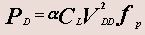 (Eq 26.12).
26.7 Methods To Reduce Dynamic Power Dissipation
As can be seen from Eq (26.12), the power dissipated can be reduced by reducing either the clock frequency,  , or the load capacitance, CL, or the rail voltage, VDD, or the switching activity parameter, α.
Reducing the clock frequency is the easiest thing to do, but it seriously affects the performance of the chip. Applications where power is paramount, this is approach can be used satisfactorily.
Another method to reduce the dissipated power is to lower the load capacitance, CL. But this method is more difficult than the previous approach because it involves conscientious system design, so that there are fewer wires, smaller pins, smaller fan-out, smaller devices etc.
Power dissipation can also be reduced by reducing the rail voltage, VDD. But this can be done only through device technology. Also rail voltage is a standard agreed to in many cases by the semiconductor industry, hence we do not have much control over this parameter. Also rail voltage is strongly dependent on the threshold voltage and the noise margin.
Some special techniques are also used to reduce power dissipation. The first one involves the use of pipelining to operate the internal logic at a lower clock than the i/o frequency. The other technique is to reduce switching activity, α, by optimizing algorithms, architecture, logic topology and using special encoding techniques.
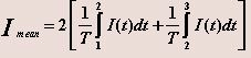
26.8 Short-Circuit Power Dissipation
The short-circuit power dissipation is given by
 (Eq 26.13)
For the input waveform shown in Fig 26.81a, which depicts the short-circuit (Fig26.81b) in an unloaded inverter,
 (Eq 26.14)
assuming that 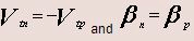 and that the behavior is symmetrical around t2.
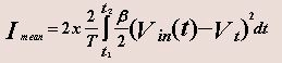
with
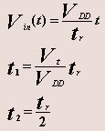
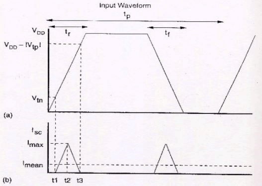
Thus for an inverter without load, assuming that 
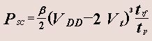
where tp is the period of the waveform. This derivation is for an unloaded inverter. It shows that the short-circuit current is dependent on β and the input waveform rise and fall times. Slow rise times on nodes can result in significant (20%) short-circuit power dissipation for loaded inverters. Thus it is good practice to keep all edges fast if power dissipation is a concern. As the load capacitance is increased the signifance of the short-circuit dissipation is reduced by the capacitive dissipation PD.
FAQs on Power Dissipation in CMOS Circuits
| 1. What is power dissipation in CMOS circuits? |  |
| 2. How is power dissipation calculated in CMOS circuits? | |
| 3. What are the factors that contribute to power dissipation in CMOS circuits? | |
| 4. How can power dissipation be reduced in CMOS circuits? | |
| 5. What are the implications of high power dissipation in CMOS circuits? | |

